PGA400-Q1
www.ti.com
SLDS186 –MARCH 2012
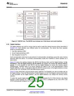
For more information on OWI protocol, operation, avaialble commands and example communication refer
to the PGA400-Q1 Programming Application Note (SLDA015).
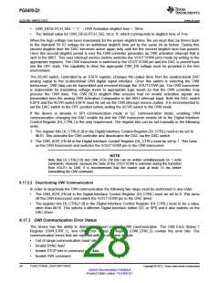
6.18 Serial Peripheral Interface (SPI) Interface
The device includes a Serial Peripheral Interface (SPI) digital communication interface. The main function
of the SPI is to enable writes to and reads from all addresses available for SPI access.
6.18.1 Overview of SPI Interface
SPI is a synchronous, serial, master-slave, communication standard that requires the following four pins:
•
•
•
•
SDI: SPI slave in master out, serial input pin.
SDO:SPI slave out master in, serial output pin (tri-state output)
SCK: SPI clock which controls the communication.
CS: chip select (active low)
SPI comminucates in a master/slave style where only one device, the master, can initiate data
transmissions. The PGA400-Q1 always acts as the slave in SPI communication, where whatever external
device that is communicating to it becomes the master mode. Both devices begin data transmission with
the most significant bit (MSB) first.
Because multiple slave devices can exist on one bus, the master node is able to notify the specific slave
node that it is ready to begin communicating with by driving the CS line to a low logic level. In the absence
of active transmission, the master SPI device places the device in reset by driving the CS pin to a high
logic level. During a reset state the SDO pin operates in tri-state mode. For the SPI interface to have
access to memory locations other than test register space, the IF_SEL bit in the Micro/Interface Control
Test register (MICRO_IF_SEL_T) has to be set to ‘1’.
6.18.2 Activating the SPI Interface
To activate SPI communication the following steps must be made in order:
1. Place the 8051W in reset by setting the MICRO_RESET bit in the Micro/Interface Control Register
(MICRO_IF_SEL_T) to logic "high"
2. Give control of the memory block to the digital interface by setting the IF_SEL bit in the Micro/Interface
Control Register (MICRO_IF_SEL_T)to logic "high"
3. Set the DI_CTRL bits in the Digital Interface Control Register (DI_CTRL) to 0b00 for SPI interface
6.18.3 Clocking Details of SPI Interface
Input data on the SDI pin must be valid on the rising edge of the SCK clock, whereas output data on the
SDO pin changes during the rising edge of the SCK clock. For SPI timing information the SPI Timing
diagram is shown in Figure 5-1.
For more information on SPI protocol, operation, avaialble commands and example communication refer
to the PGA400-Q1 Programming Application Note (SLDA015).
6.19 Inter-Integrated Circuit Interface
The device includes an Inter-Integrated Circuit (I2C) digital communication interface. The main function of
the I2C is to enable writes to, and reads from, all addresses available for I2C access.
6.19.1 Overview of I2C Interface
I2C is a synchronous serial communication standard that requires the following two pins for
communication:
•
•
GPIO_1/IC_1/SDA: I2C Serial Data Line (SDA)
GPIO_3/OC_1/SCL: I2C Serial Clock Line (SCL)
Copyright © 2012, Texas Instruments Incorporated
FUNCTIONAL DESCRIPTIONS
29
Submit Documentation Feedback
Product Folder Link(s): PGA400-Q1

 TI [ TEXAS INSTRUMENTS ]