PGA400-Q1
SLDS186 –MARCH 2012
www.ti.com
•
•
OWI_DEGLITCH_SEL = ‘1’ → OWI Activation deglitch time = 10ms
The default value for OWI_DEGLITCH_SEL bit is ‘0’, which corresponds to deglitch time of 1ms.
When the high voltage has been maintained for the proper deglitch time, the pin must then be driven back
to the standard 5V IO voltage for an additional deglitch time set by the same bit as before. During this
second deglitch time the DAC becomes active again only until the the second deglitch time has passed.
Once this second deglitch period is over the OWI controller generates an OWI activation interrupt that is
sent to the 8051. This user interrupt service routine switches the VOUT1/OWI pin's mode by writing to the
appropriate registers. The OWI transceiver is switched to the VOUT1/OWI pin and the DAC is placed back
into the OFF state. The capability to drive the appropiate OWI_EN voltage must be provided in the test
environment.
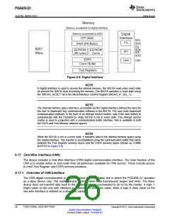
The XCVR switch, controlled by an ESFR register, changes the output drive from the unidirectional DAC
analog signal to the bi-directional OWI digital signal interface. Once this switch is selecting the OWI
transceiver, OWI data can be transmitted and received through the VOUT1/OWI pin. The OWI transceiver
is responsible for translating voltage levels to appropriate logic levels so that the OWI controller may
process the OWI data. The OWI_REQ deglitch filter ensures that no invalid activation signals are
transmitted from the analog OWI Activation Comparator to the 8051 interrupt input. Both the DAC switch
ESFR and the XCVR switch ESFR must be set via the OWI interrupt service routine. It is recommended to
set the DAC switch to the OFF position before setting the XCVR switch to the OWI mode.
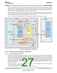
If the device is already in SPI communication mode or I2C communication mode, enabling OWI
communication changing the DAC enable bit and the OWI transceiver enable bit in the Digital Interface
Control Register (DI_CTRL) is the only requirement. The register bits can be set manually in the following
order.
1. The register bits DI_CTRL[1:0] in the Digital Interface Control Register (DI_CTRL) need to be set to
0b10. This activates the OWI controller and deactivates the DAC via the DAC switch.
2. The OWI_XCR_EN bit in the Digital Interface Control Register (DI_CTRL) must be set to 1. This turns
on the OWI transceiver and switches the VOUT1/OWI pin to the OWI transceiver.
NOTE
Note that DI_CTRL[1:0] and OWI_XCR_EN bits can be written simultaneously (in 1 write
command). However, because the state of the VOUT1/OWI is unknown during the transition
from VOUT1 to OWI, it is recommended that the master wait at least 15 ms before
transmitting the OWI command.
6.17.2.2 Deactivating OWI Communication
In order to deactivate the OWI communication the following two steps must be performed in any order.
•
The OWI_XCR_EN bit in the Digital Interface Control Register (DI_CTRL) must be set to 0. This turns
off the OWI transceiver and switch the VOUT1/OWI pin to the DAC driver.
•
The register bits DI_CTRL[1:0] in the Digital Interface Control Register (DI_CTRL) must to be a value
other than 0b10. This selects a different Digital Interface (either I2C or SPI) and it also switchs on the
DAC driver.
6.17.3 OWI Communication Error Status
The device has the ability to detect and report errors in OWI communication. The OWI Error Status 1
Register (OWI_ERR_1), and OWI Error Status 2 Register (OWI_ERR_2) contain the error bits. The
communication errors that are reported with the registers include
•
•
•
•
Out of range communication baud rate
Invalid SYNC field
Invalid STOP bits in command and data
Invalid OWI command
28
FUNCTIONAL DESCRIPTIONS
Copyright © 2012, Texas Instruments Incorporated
Submit Documentation Feedback
Product Folder Link(s): PGA400-Q1

 TI [ TEXAS INSTRUMENTS ]