PGA400-Q1
www.ti.com
SLDS186 –MARCH 2012
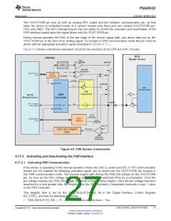
The VOUT1/OWI pin acts as both an analog DAC output and the interface communication pin, so that
when the device is embedded inside of a system module only three pins are needed (VOUT1/OWI pin,
VDD and GND). The 8051 microprocessor has the ability to control the activation and deactivation of the
OWI interface based upon the signal driven into the VOUT1/OWI pin.
During normal operation the DAC is the last stage of the sensor signal path, and drives data out on the
VOUT1/OWI pin in the form of an analog signal. To change to OWI communication mode this pin must be
driven with an appropiate activation signal described in Section 6.17.2.
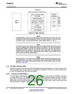
Figure 6-9 shows a functional equivalent circuit for the structure of the OWI and DAC circuitry.
Figure 6-9. OWI System Components
6.17.2 Activating and Deactivating the OWI Interface
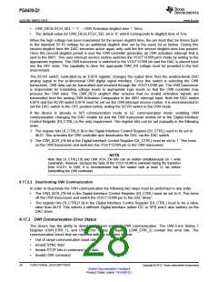
6.17.2.1 Activating OWI Communication
If the device is operating in the normal operation where the DAC is active and I2C or SPI communication
modes are not enabled the following activation signal can be driven into the VOUT1/OWI pin to place it
into OWI communication mode. The process begins with driving the OWI_EN voltage on the VOUT1/OWI
pin. As soon as the DAC voltage exceeds 5.4 volts the DAC is switched off by by a comparator. Once the
pin voltage reaches the OWI_EN voltage threshold a deglitch timer begins. Once the pin voltage has been
asserted for a time greater than the deglitch time the OWI Activation Comparator transmits a logic 1 value
to the OWI Controller.
This deglitch time is set by the OWI_DEGLITCH_SEL bit in the Digital Interface Control Register
(DI_CTRL), and has the following properties:
•
OWI_DEGLITCH_SEL = ‘0’ → OWI Activation deglitch time = 1ms
Copyright © 2012, Texas Instruments Incorporated
FUNCTIONAL DESCRIPTIONS
27
Submit Documentation Feedback
Product Folder Link(s): PGA400-Q1

 TI [ TEXAS INSTRUMENTS ]