PGA400-Q1
www.ti.com
SLDS186 –MARCH 2012
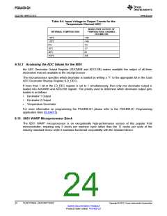
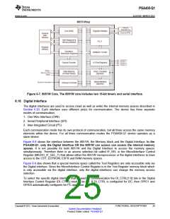
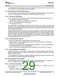
Figure 6-7. 8051W Core. The 8051W core includes two 16-bit timers and serial interface.
6.16 Digital Interface
The digital interfaces are used to access (read as well as write) the internal memory spaces described in
Section 6.20. Each interface uses different pin(s) for communication. The device has three separate
modes of communication:
1. One-Wire Interface (OWI)
2. Serial Peripheral Interface (SPI)
3. Inter-Integrated Circuit (I2C)
Each communication mode has its own protocol of communication, but all three access the same memory
elements within the device. For all three communication modes the PGA400-Q1 device operates as a
slave device.
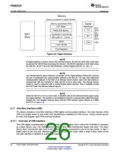
Figure 6-8 shows the interface between the 8051W, the Memory block and the Digital Interface. In the
PGA400-Q1, only the Digital Interface OR the 8051W can access can access the internal memory
spaces. It is not possible for both 8051W and the Digital Interface to access the memory spaces
simultaneously. Therefore there is an access selection bit called IF_SEL in the Micro/Interface Control
Register (MICRO_IF_SEL_T) that allows either the 8051W microprocessor or the digital interfaces to have
access to the OTP, EEPROM, ESFR and RAM memory spaces.
Figure 6-8 also shows that a special memory space called the Test Registers are only accessible only via
the Digital interface. Since the Micro/Interface Control Register is in the Test Register memory block which
is only accessible via the digital interface, only the digital interfaces can change the memory access
selection.
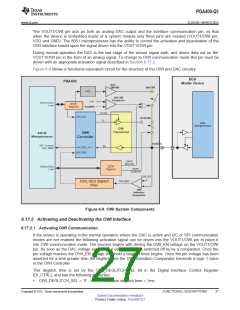
To select the specific digital interface that is used for communication the DI_CTRL[1:0] bits in the Digital
Interface Control Register (DI_CTRL) need to be set. If DI_CTRL is configured for I2C, then GPIO1 and
GPIO3 automatically configures for I2C operation.
Copyright © 2012, Texas Instruments Incorporated
FUNCTIONAL DESCRIPTIONS
25
Submit Documentation Feedback
Product Folder Link(s): PGA400-Q1

 TI [ TEXAS INSTRUMENTS ]