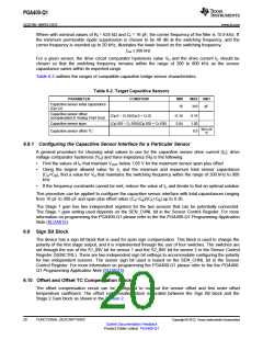
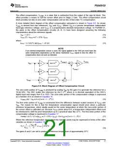
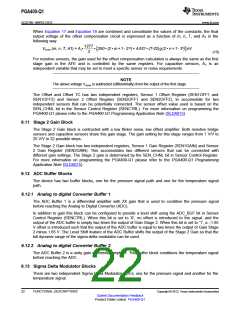
PGA400-Q1
SLDS186 –MARCH 2012
www.ti.com
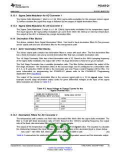
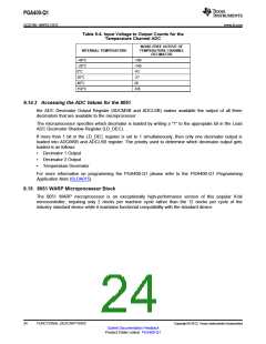
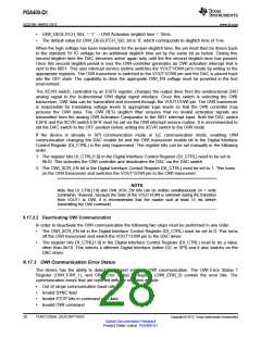
Table 6-4. Input Voltage to Output Counts for the
Temperature Channel ADC
NOISE-FREE OUTPUT OF
INTERNAL TEMPERATURE
–40°C
TEMPERATURE CHANNEL
DECIMATOR
-196
–20°C
0°C
-140
-83
-27
28
20°C
40°C
150°C
338
6.14.3 Accessing the ADC Values for the 8051
the ADC Decimator Output Register (ADCMSB and ADCLSB) makes available the output of all three
decimators that are available to the microprocessor.
The microprocessor specifies which decimator is loaded by writing a "1" to the appropiate bit in the Load
ADC Decimator Shadow Register (LD_DEC).
If more than 1 bit in the LD_DEC register is set to 1 simultaneously, then only one decimator output is
loaded into ADCMSB and ADCLSB register. The priority used to determine which decimator output gets
loaded is as follows:
•
•
•
Decimator 1 Output
Decimator 2 Output
Temperature Decimator
For more information on programming the PGA400-Q1 please refer to the PGA400-Q1 Programming
Application Note (SLDA015).
6.15 8051 WARP Microprocessor Block
The 8051 WARP microprocessor is an exceptionally high-performance version of this popular 8-bit
microcontroller, requiring only 2 clocks per machine cycle rather than the 12 clocks per cycle of the
industry standard device while it maintains functional compatibility with the standard device
24
FUNCTIONAL DESCRIPTIONS
Copyright © 2012, Texas Instruments Incorporated
Submit Documentation Feedback
Product Folder Link(s): PGA400-Q1

 TI [ TEXAS INSTRUMENTS ]