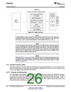
PGA400-Q1
SLDS186 –MARCH 2012
www.ti.com
When Equation 17 and Equation 18 are combined and consolidate the values of the constants, the final
output voltage of the offset compensation circuit is expressed as a function of m, n, T, and A1 in the
following way:
1277
Vcomp (m, n, T, A1) = A •
• 250 • (2 • m +1 - 210)+ 4.921 • (T-22)g (2 • n +1 - 26) nV
[
]
1
3
(19)
For resistive sensors, the gain used for the offset compensation calculation is always the same as the first
stage gain in the AFE and is controlled by the same registers. For capacitive sensors, A1 is an
independent variable that may be set to meet a specific sensor or noise requirements.
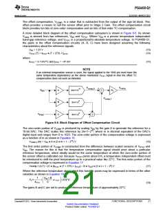
NOTE
The above voltage Vcomp is subtracted (differentially) from the output of the first stage.
The Offset and Offset TC has two independent registers, Sensor 1 Offset Register (SEN1OFF1 and
SEN1OFF2) and Sensor 2 Offset Register (SEN2OFF1 and SEN2OFF2), to accomodate for two
independent sensors that can be potentially connected. The sensor offset value used is based on the
SEN_CHNL bit in the Sensor Control Register (SENCTRL). For more information on programming the
PGA400-Q1 please refer to the PGA400-Q1 Programming Application Note (SLDA015).
6.11 Stage 2 Gain Block
The Stage 2 Gain block is contructed with a low flicker noise, low offset amplifier. Both resistive bridge
sensors and capacitive sensors share this gain stage. The gain setting for this stage ranges from 1 V/V to
25 V/V in 32 possible steps.
The Stage 2 Gain block has two independent registers, Sensor 1 Gain Register (SEN1GAIN) and Sensor
2 Gain Register (SEN2GAIN). This accomodates two different sensors that can be connected with
different gain settings. The Stage 2 gain is determined by the SEN_CHNL bit in Sensor Control Register.
For more information on programming the PGA400-Q1 please refer to the PGA400-Q1 Programming
Application Note (SLDA015).
6.12 ADC Buffer Blocks
The device has two buffer blocks, one for the pressure signal path and one for the temperature signal
path.
6.12.1 Analog to digital Converter Buffer 1
The ADC Buffer 1 is a differential amplifier with 2X gain that is used to condition the pressure signal
before reaching the Analog to Digital Converter (ADC).
In addition to gain this block can be configured to provide a level shift using the ADC_BUF bit in Sensor
Control Register (SENCTRL). When this bit is set to ‘0’, no offset is introduced to the signal, and the
output of the ADC buffer is simply two times the output of Gain Stage 2. When this bit is set to ‘1’, a –1.65
V offset is introduced such that the output of the ADC buffer is equal to two times the output of Gain Stage
2 minus 1.65 V. The Level Shift feature of the ADC Buffer shifts the output of the Stage 2 Gain so that the
full dynamic range of the sigma-delta modulator can be used.
6.12.2 Analog to digital Converter Buffer 2
The ADC Buffer 2 is a unity gain differential amplifier. This buffer block conditions the temperature signal
before reaching the ADC.
6.13 Sigma Delta Modulator Blocks
There are two independent Sigma Delta Modulator ADCs, one for the pressure signal and another for the
temperature signal.
22
FUNCTIONAL DESCRIPTIONS
Copyright © 2012, Texas Instruments Incorporated
Submit Documentation Feedback
Product Folder Link(s): PGA400-Q1

 TI [ TEXAS INSTRUMENTS ]