PGA400-Q1
www.ti.com
SLDS186 –MARCH 2012
The offset compensation, VCOMP, is a value that is subtracted from the output of the sign bit block. This
offset provides a means to null the sensor offset prior to Stage 2 Gain. The offset compensation circuit
block provides ten bits of zero-order compensation and six bits of first-order TC compensation.
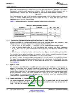
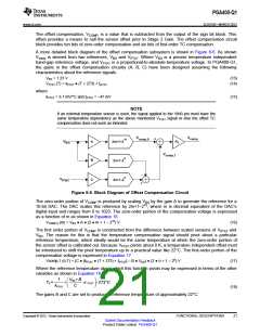
A more detailed block diagram of the offset compensation subsystem is shown in Figure 6-6. As shown
Vcomp is derived from two references, VBG and VPTAT. Where VBG is a precise temperature independent
band-gap reference voltage, and VPTAT is a proportional-to-absolute-temperature voltage. In PGA400-Q1,
the gains in the offset compensation circuitry (A, B, C) have been designed assuming the following
characteristics about the reference signals:
VBG = 1.23 V
(13)
(14)
VPTAT (T) = kPTAT ● (T + 273) + ξPTAT
where
kPTAT = 3.7 mV/°C and ξPTAT = –47 mV
(15)
NOTE
If an external temperature sensor is used, the signal applied to the VIN3 pin must have the
same temperature dependency as the above mentioned VPTAT signal or else the offset TC
compensation does not work as intended.
V
V
+
comp
comp,0
10
V
A
1
A
B
2m+1-2
BG
-
V
comp,1
6
2n+1-2
2n+1-2
-
6
V
C
PTAT
+
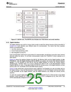
Figure 6-6. Block Diagram of Offset Compensation Circuit
The zero-order portion of VCOMP is produced by scaling VBG by the gain A to generate the reference for a
10-bit DAC. The DAC scales this reference by 2m+1–210, where m is decimal equivalent of the DAC’s
digital input and ranges from 0 to 1023. The zero-order portion of the compensation voltage is expressed
as a function of m as shown in Equation 16.
VCOMP,0 (m) = VBG ● A ● (2 ● m + 1 – 210) V
(16)
The first order portion of VCOMP is constructed from the difference between scaled versions of VPTAT and
VBG. The reason for this is that the temperature compensation signal should pivot about a particular
reference temperature, which ideally would be the same temperature at which the zero-order portion of
the sensor offset is calibrated out. Because VPTAT pivots about 0 K, a temperature independent offset must
be introduced to shift the pivot temperature up to a practical value like 22°C. The first-order portion of the
compensation voltage is expressed in Equation 17.
Vcomp,1 (n,T) = (C ● [kPTAT ● (T + 273) + ξPTAT] – B ● VBG) ● (2 ● n + 1 – 26) V
(17)
Where the reference temperature about which this function pivots may be expressed in terms of the other
variables as shown in Equation 18.
1
V
BG • B
æ
ç
è
ö
÷
ø
TR =
•
-ε
-273°C
PTAT
kPTAT
C
(18)
The gains B and C are set to produce a reference temperature of approximately 22°C.
Copyright © 2012, Texas Instruments Incorporated
FUNCTIONAL DESCRIPTIONS
21
Submit Documentation Feedback
Product Folder Link(s): PGA400-Q1

 TI [ TEXAS INSTRUMENTS ]