PGA400-Q1
SLDS186 –MARCH 2012
www.ti.com
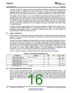
Where with nominal values of Rf = 625 kΩ and Cf = 16 pF, the corner frequency of the filter is 15.9 kHz. If
the minimum permissible ripple suppression is chosen to be 40 dB at the switching frequency, and the
corner frequency is rounded up to 20 kHz, illustrates the lower bound on the switching frequency:
ƒmin ≥ 200 kHz
For a given sensor, the drive circuit comparator hysteresis value VH and the drive current IC should be
chosen so that the switching frequency remains within the range of 200 to 800 kHz as the sensor
capacitance varies within its expected range.
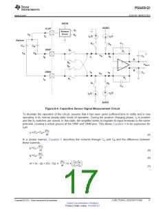
Table 6-2 outlines the ranges of compatible capacitive bridge sensor characteristics.
Table 6-2. Target Capacitive Sensors
PARAMETER
CONDITION
MIN
MAX UNIT
Capacitive sensor initial capacitance
(Cp+Cr)
10
310
pF
Capacitive sensor offset
(compensated in Analog Front End)
(Cp,0 – Cr,0)/(Cp,0 + Cr,0)
–0.16
0.04
0.16
1.00
0.8
Capacitive sensor span
(Cp,100 – Cr,100)/(Cp,100 + Cr,100)
%Cv,0/
°C
Capacitive sensor offset TC
6.8.1 Configuring the Capacitive Sensor Interface for a Particular Sensor
A general procedure for choosing what values to use for the capacitive sensor drive current (IC), drive
voltage comparator hysteresis (VH) and trans-impedance (Rf) is the following:
•
•
Find the values of IC that maintain VOUT below 1.65 V for the maximum sensor span plus offset
Using the largest allowed value for IC and the minimum and maximum total sensor capacitance
(CA+CB), find a value for VH that maintains the switching frequency within the range of 200 kHz to 800
kHz
•
If the frequency constraints cannot be met, reduce the value of IC and iterate to find an optimal solution
This procedure can be applied to configure the capacitive sensor interface with total capacitances ranging
from 10 pF to 300 pF and span plus offset ratios (CA–CB)/(CA+CB) up to 0.36.
The Stage 1 gain has two independent registers for the two sensors that can be potentially connected.
The Stage 1 gain setting used depends on the SEN_CHNL bit in the Sensor Control Register. For more
information on programming the PGA400-Q1 please refer to the the PGA400-Q1 Programming Application
Note (SLDA015).
6.9 Sign Bit Block
The device has a sign bit block that is used for span sign compensation. This block is used to change the
polarity of the first stage output, and it is implemented through the use of four switches. The switches are
set through the use of the S1_INV bit for sensor 1 and the S2_INV bit for sensor 2 in the Sensor Control
Register (SENCTRL). There are two independent sign bit settings to accommodate configuring the polarity
for two independent sensors. The sensor sign bit used is based on the SEN_CHNL bit in the Sensor
Control Register. For more information on programming the PGA400-Q1 please refer to the the PGA400-
Q1 Programming Application Note (SLDA015).
6.10 Offset and Offset TC Compensation Blocks
The offset compensation circuit can be configured to null out the sensor offset and first order offset
temperature coefficient. The offset compensation block is located between the Sign Bit block and the
Stage 2 Gain block as shown in the Section 2.
20
FUNCTIONAL DESCRIPTIONS
Copyright © 2012, Texas Instruments Incorporated
Submit Documentation Feedback
Product Folder Link(s): PGA400-Q1

 TI [ TEXAS INSTRUMENTS ]