PGA400-Q1
SLDS186 –MARCH 2012
www.ti.com
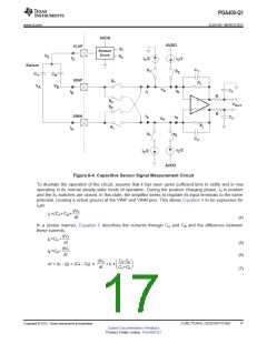
The drive current is split between the capacitors in proportion to their relative difference. Measuring ΔI
provides a means to infer the value of the difference in capacitance (CA – CB) or the value of one of the
capacitors if the other is known. Also, driving the sensor with a current source and measuring the resulting
difference in current has the benefit of being fully differential and thus less susceptible to common-mode
disturbances and non-idealities. Note that the expressions for IA and IB may are rewritten in terms of
common-mode and differential-mode components in Equation 8 and Equation 9.
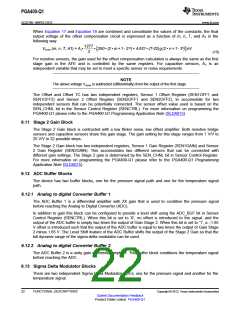
IX
2
IX
2
ΔI
IA=
+
2
(8)
ΔI
2
IB =
-
(9)
The capacitive sensor signal measurement circuit extracts and amplifies ΔI. Figure 6-5 illustrates the
current waveforms at different points in the circuit of Figure 6-4. The currents into and out of the sensor
are shown on axis (a). Initially, the circuit is in the discharge phase where IX is negative and S2 switches
are closed. After some time, the state switches to the charge phase where the S1 switches are closed.
This process of changing the state of the circuit continues periodically with a frequency set by the sensor
drive circuit.
During each half cycle the IX current is split into the individual capacitor currents IA and IB. As shown in
Figure 6-5(b), while the S1 switches are closed I2 = IA and I1 = IB, but when the S2 switches are closed the
currents are inverted such that I2 = IB and I1 = IA. Because the sign of IX is also changing, the difference
between I2 and I1 remains constant and equal to ΔI (ignoring the glitches that occur at phase transitions).
While the S1 switches are closed, half the sensor drive current (IC/2) is subtracted from I2 and I1 and while
the S2 switches are closed, half the sensor drive current is added to them. This removes the cycle-to-cycle
offset in Figure 6-5(b), delivering the DC currents IP and IN to the trans-impedance amplifier, as shown in
Figure 6-5(c) where IP – IN = ΔI. For low frequency signals, the output voltage of the amplifier is shown in
Equation 10.
æ
ç
è
ö
÷
ø
CA -CB
CA+ CB
Vout = R •ΔI = R • I C•
ò
ò
(10)
For a given sensor, the drive current IC should be adjusted to keep VOUT < 1.65 V over the expected
operating conditions of the sensor to avoid saturating the ADC input.
NOTE
for some types of wide span sensors, it may be necessary to reduce the gain set by the
value of Rf in the transimpedance amplifier. The drive current IC and feedback resistance Rf
can be adjusted via Capacitive Sensor Settings Register (CAPSEN). For more information on
programming the PGA400-Q1 please refer to the PGA400-Q1 Programming Application Note
(SLDA015).
18
FUNCTIONAL DESCRIPTIONS
Copyright © 2012, Texas Instruments Incorporated
Submit Documentation Feedback
Product Folder Link(s): PGA400-Q1

 TI [ TEXAS INSTRUMENTS ]