PGA400-Q1
SLDS186 –MARCH 2012
www.ti.com
The SEN_TYP bit of the Capacitive Sensor Settings Register (CAPSEN) configures the device to be used
with either resisitive or capacitve sensor types. When this bit is set to ‘0’, the device is configured for
capacitive sensors and when the bit is set to "1" the device is configured for resistive bridge sensors.
When either front-end is selected, the other option is disabled and placed in a low quiescent current state.
The Analog Front End (AFE) can also be configured to measure two sensors sequentially. This is
controlled via the SEN_CHNL bit in the Sensor Control Register (SENCTRL). When this bit is set to ‘0’,
the analog MUX at the input of the AFE is switched to pass the signals present at VIN1P and VIN1N pins.
For capacitive sensors, the capacitive sensor drive current is also applied to the ICAP1 pin. When this bit
is set to ‘1’, the VIN2P, VIN2N and ICAP2 pins become active. The SEN_CHNL bit also controls which
External Special Function Registers (ESFRs) are applied to the Stage 1 Gain, Stage 2 Gain, Offset, Offset
TC and the Sign bits.
In addition the sensor supply regulator can be independently enabled or disabled via the VBRG_EN bit in
the Sensor Control Register (SENCTRL). This allows the VBRG 3.3 V output to be used with external
temperature sensors while the AFE is configured in capacitive sensor mode. For more information on
programming the PGA400-Q1 please refer to the
6.7 Stage 1 Gain Block
When the device is configured to interface with resistive sensors, the first gain block that the signal passes
through in the AFE is the Stage 1 Gain block. This gain block is designed with precision, low drift, low
flicker noise amplifiers.
The gain of this stage is adjustable to accommodate sensors with a wide-range of signal spans and can
be set from 3V/V to 51V/V in 8 possible steps. The Stage 1 Gain has two independent registers, Sensor 1
Gain Register (SEN1GAIN) and Sensor 2 Gain Register (SEN2GAIN), so that two different resistive
sensors can be connected with different gain settings. For Stage 1 Gain settings use either the S1_G1 bits
or the S2_G2 bits in the registers mentioned above. The gain setting that is used depends on the
SEN_CHNL bit in Sensor Control Register (SENCTRL). For more information on programming the
PGA400-Q1 please refer to the PGA400-Q1 Programming Application Note (SLDA015).
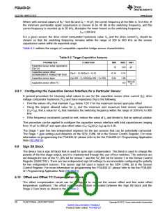
Table 6-1 outlines the ranges of of resistive bridge sensor characteristics that are compatible.
Table 6-1. Target Resistive Bridge Sensors
PARAMETER
CONDITION
–40°C ≤ TA ≤ 150°C
MIN
2
TYP
MAX
UNIT
Resistive bridge resistance
Resistive bridge resistance TC
20
KΩ
–350
4800 PPM/°C
33 mV/V
40 µV/V/°C
75 mV/V
Resistive bridge offset
(compensated in Analog Front End)
TA = 25°C
–33
Resistive bridge offset TC
(compensated in Analog Front End)
–40
1.4
Resistive bridge span
TA = 25°C
6.8 Self Oscillating Demodulator Block
Figure 6-4 shoes an essential schematic of the capacitive sensor signal measurement circuit. . The
Sensor Voltage Supply block discussed in is depicted only as a functional block called Sensor Drive that
provides the sensor drive current via the ICAPx pin and the clock signals S1 and S2 that are used by the
synchronous demodulator in the measurement circuit. As with the ICAP supply circuitry the demodulator
block circuitry toggles between two states during normal operation. In one state the S1 switches are closed
while the S2 switches are open and in the other state the S1 switches are open while the S2 switches are
closed.
16
FUNCTIONAL DESCRIPTIONS
Copyright © 2012, Texas Instruments Incorporated
Submit Documentation Feedback
Product Folder Link(s): PGA400-Q1

 TI [ TEXAS INSTRUMENTS ]