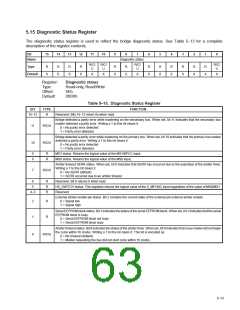
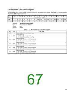
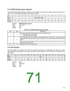
5.19 Secondary Clock Control Register
The secondary clock control register is used to control the secondary clock outputs. See Table 5–17 for a complete
description of the register contents.
Bit
15
14
13
12
11
10
9
8
7
6
5
4
3
2
1
0
Name
Type
Default
Secondary clock control
R
0
R
0
R
0
R
0
R
0
R
0
R
0
R/W
0
R/W
0
R/W
0
R/W
0
R/W
0
R/W
0
R/W
0
R/W
0
R/W
0
Register:
Type:
Secondary clock control
Read-only, Read/Write
Offset:
Default:
68h
0000h
Table 5–17. Secondary Clock Control Register
BIT
TYPE
FUNCTION
15–9
R
Reserved. Bits 15–9 return 0s when read.
Clockout4 disable.
8
R/W
0 = Clockout4 enabled (default)
1 = Clockout4 disabled and driven high
Clockout3 disable.
7–6
5–4
3–2
1–0
R/W
R/W
R/W
R/W
00, 01, 10 = Clockout3 enabled (00 default)
11 = Clockout3 disabled and driven high
Clockout2 disable.
00, 01, 10 = Clockout2 enabled (00 default)
11 = Clockout2 disabled and driven high
Clockout1 disable.
00, 01, 10 = Clockout1 enabled (00 default)
11 = Clockout1 disabled and driven high
Clockout0 disable.
00, 01, 10 = Clockout0 enabled (00 default)
11 = Clockout0 disabled and driven high
5–17

 TI [ TEXAS INSTRUMENTS ]