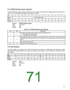
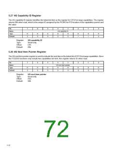
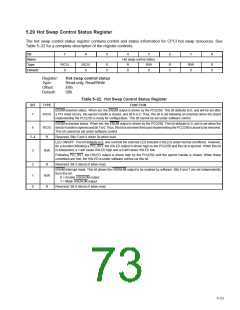
5.25 PMCSR Bridge Support Register
The PMCSR bridge support register is required for all PCI bridges and supports PCI bridge specific functionality. See
Table 5–21 for a complete description of the register contents.
Bit
7
6
5
4
3
2
1
0
Name
Type
Default
PMCSR bridge support
R
X
R
X
R
0
R
0
R
0
R
0
R
0
R
0
Register:
Type:
Offset:
Default:
PMCSR bridge support
Read-only
E2h
X0h
Table 5–21. PMCSR Bridge Support Register
BIT
TYPE
FUNCTION
Bus power control enable. This bit returns the value of the MS1/BCC input.
0 = Bus power/ clock control disabled
7
R
1 = Bus power/clock control enabled
B2/B3 support for D3 . This bit returns the value of MS1/BCC input. When this bit is 1, the secondary clocks
hot
are stopped when the device is placed in D3 . When this bit is 0, the secondary clocks remain on in all device
hot
states.
6
R
R
Note: If the primary clock is stopped, then the secondary clocks will stop because the primary clock is used to
generate the secondary clocks.
5–0
Reserved. Bits 5–0 return 0s when read.
5.26 Data Register
The data register is an optional, 8-bit read–only register that provides a mechanism for the function to report
state-dependent operating data such as power consumed or heat dissipatin. The PCI2050 does not implement the
data register.
Bit
7
6
5
4
3
2
1
0
Name
Type
Default
Data
R
0
R
0
R
0
R
0
R
0
R
0
R
0
R
0
Register:
Type:
Offset:
Default:
Data
Read-only
E3h
00h
5–21

 TI [ TEXAS INSTRUMENTS ]