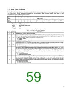
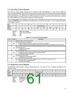
5.13 Clock Run Control Register
The clock run control register controls the PCI clock-run mode enable/disable. It is also used to enable the
keep-clock-running feature. Bit 0 reflects the status of the secondary clock. There are two clock run modes supported
on the secondary bus. The bridge can be configured to stop the secondary PCI clock only in response to a request
from the primary bus to stop the clock or it can be configured to stop the secondary clock whenever the secondary
bus is idle and there are no transaction requests from the primary bus.
There are two conditions for restarting the secondary clock. A downstream transaction restarts the secondary clock,
or if the S_CLKRUN signal is asserted, the secondary clock is restarted. See Table 5–11 for a complete description
of the register contents.
Bit
7
6
5
4
3
2
1
0
Name
Type
Default
Clock run control
R/W R/W
R
0
R
0
R
0
R/W
0
R/W
0
R
0
0
0
Register:
Type:
Clock run control
Read-only, Read/Write
Offset:
Default:
5Bh
00h
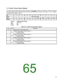
Table 5–11. Clock Run Control Register
BIT
TYPE
FUNCTION
7–5
R
Reserved. Bits 7–5 return 0s when read.
Clock run mode. Bit 4 is encoded as:
0 = Stop the secondary clock only on request from the primary bus (default).
4
3
R/W
1 = Stop the secondary clock whenever the secondary bus is idle and there are no requests from the primary bus.
Primary clock run enable. Bit 3 must be enabled for the bridge to respond to requests by the central resource on the primary
bus to stop the clock.
R/W
0 = Disable clock run (default)
1 = Enable clock run
Primary keep clock. When bit 2 is set, it causes the bridge to request that the central resource keep the PCI clock running.
0 = Allow primary clock to stop if secondary clock stopped (default)
2
1
0
R/W
R/W
R
1 = Always keep primary clock running
Secondary clock run enable
0 = Disable clock run for secondary (default)
1 = Enable clock run for secondary
Secondary clock status bit. If the clock is stopped, this bit is 1. If the clock is running, this bit is 0.
0 = Secondary clock not stopped (default)
1 = Secondary clock stopped
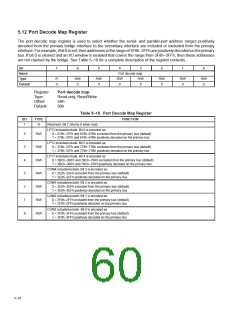
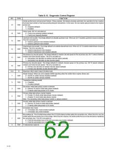
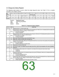
5.14 Diagnostic Control Register
The diagnostic control register is used for bridge diagnostics. See Table 5–12 for a complete description of the
register contents.
Bit
15
14
13
12
11
10
9
8
7
6
5
4
3
2
1
0
Name
Type
Default
Diagnostic control
R/W
0
R/W
0
R/W
0
R/W
1
R/W
0
R/W
0
R
0
R
0
R/W
0
R/W
1
R/W
0
R/W
0
R/W
0
R/W
0
R/W
0
R/W
0
Register:
Type:
Offset:
Default:
Diagnostic control
Read/Write, Read-only
5Ch–5Dh
1040h
5–11

 TI [ TEXAS INSTRUMENTS ]