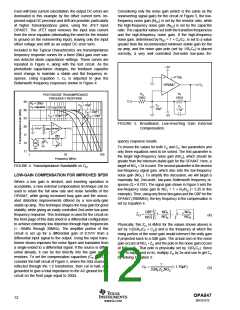
practice, this only holds true when the phase margin ap-
proaches 90°, as it does in high-gain configurations. At low
gains (increased feedback factors), most high-speed ampli-
fiers exhibit a more complex response with lower phase
margin. The OPA847 is compensated to give a maximally flat
2nd-order Butterworth closed-loop response at a noninverting
gain of +20 (see Figure 1). This results in a typical gain of
+20 bandwidth of 350MHz, far exceeding that predicted by
dividing the 3900MHz GBP by 20. Increasing the gain causes
the phase margin to approach 90° and the bandwidth to more
closely approach the predicted value of (GBP/NG). At a gain
of +50, the OPA847 very nearly matches the 78MHz band-
width predicted using the simple formula and the typical GBP
of 3900MHz.
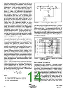
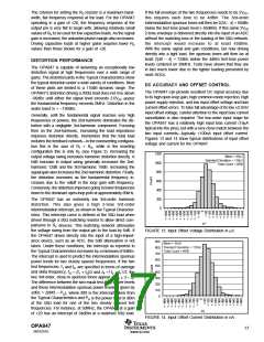
ENI
EO
OPA847
RS
IBN
ERS
RF
√4kTRS
√4kTRF
IBI
RG
4kT
RG
4kT = 1.6E – 20J
at 290°K
FIGURE 12. Op Amp Noise Analysis Model.
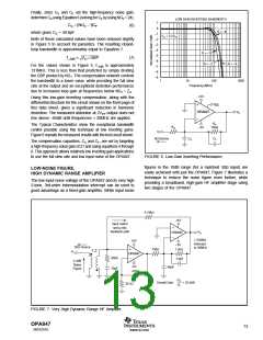
Inverting operation offers some interesting opportunities to
increase the available GBP. When the source impedance is
matched by the gain resistor (see Figure 2), the signal gain
is (1 + RF/RG), while the noise gain for bandwidth purposes
is (1 + RF/2RG). This cuts the noise gain almost in half,
increasing the minimum operating gain for inverting opera-
tion under these condition to –22 and the equivalent gain
bandwidth product to > 7.8GHz.
root to get back to a spot noise voltage. Equation 9 shows the
general form for this output noise voltage using the terms
illustrated in Figure 11.
(9)
2
2
EO
=
E2 + IBNRS + 4kTRS NG2 + I R
+ 4kTRFNG
(
)
(
)
(
)
NI
BI
F
Dividing this expression by the noise gain (NG = 1 + RF/RG)
gives the equivalent input-referred spot noise voltage at the
noninverting input, as shown in Equation 10.
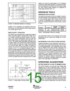
DRIVING CAPACITIVE LOADS
One of the most demanding, and yet very common, load
conditions for an op amp is capacitive loading. Often, the
capacitive load is the input of an ADC, including additional
external capacitance that may be recommended to improve
ADC linearity. A high-speed, high open-loop gain amplifier
like the OPA847 can be very susceptible to decreased
stability and may give closed-loop response peaking when a
capacitive load is placed directly on the output pin. When the
amplifier’s open-loop output resistance is considered, this
capacitive load introduces an additional pole in the signal
path that can decrease the phase margin. Several external
solutions to this problem are suggested. When the primary
considerations are frequency response flatness, pulse re-
sponse fidelity, and/or distortion, the simplest and most
effective solution is to isolate the capacitive load from the
feedback loop by inserting a series isolation resistor between
the amplifier output and the capacitive load. This does not
eliminate the pole from the loop response, but rather shifts it
and adds a zero at a higher frequency. The additional zero
acts to cancel the phase lag from the capacitive load pole,
thus increasing the phase margin and improving stability.
(10)
2
IBIRF
NG
4kTRF
NG
2
EN
=
EN2I + IBNRS + 4kTRS
+
+
(
)
Putting high resistor values into Equation 10 can quickly
dominate the total equivalent input-referred noise. A 45Ω
source impedance on the noninverting input adds a Johnson
voltage noise term equal to the amplifier’s voltage noise by
itself. As a simplifying constraint, set RG = RS in Equation 10
and assume an RS/2 source impedance at the noninverting
input, where RS is the signal source impedance and another
matching RS to ground is at the noninverting input. This
results in Equation 11, where NG > 12 is assumed to further
simplify the expression.
5
4
3RS
2
EN = EN2I
+
I R 2 + 4kT
B
S
(
)
(11)
Evaluating this expression for RS = 50Ω gives a total equiva-
lent input noise of 1.4nV/√Hz. Note that at these higher
gains, the simplified input referred spot noise expression of
Equation 11 does not include the gain. This is a good
approximation for NG > 12, as is typically required by stability
considerations.
The Typical Characteristics help the designer pick a recom-
mended RS versus capacitive load. The resulting frequency
response curves show a flat response for several selected
capacitive loads and recommended RS combinations. Para-
sitic capacitive loads greater than 2pF can begin to degrade
the performance of the OPA847. Long PCB traces, un-
matched cables, and connections to multiple devices can
easily cause this value to be exceeded. Always consider this
effect carefully and add the recommended series resistor as
close as possible to the OPA847 output pin (see the Board
Layout section).
FREQUENCY RESPONSE CONTROL
Voltage-feedback op amps exhibit decreasing closed-loop
bandwidth as the signal gain is increased. In theory, this
relationship is described by the Gain Bandwidth Product
(GBP) shown in the Electrical Characteristics. Ideally, divid-
ing GBP by the noninverting signal gain (also called the
Noise Gain, or NG) predicts the closed-loop bandwidth. In
OPA847
16
SBOS251E
www.ti.com

 TI [ TEXAS INSTRUMENTS ]