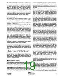
The shutdown feature for the OPA847 is a positive-supply
referenced, current-controlled interface. Open-collector (or drain)
interfaces are most effective, as long as the controlling logic
can sustain the resulting voltage (in open mode) that appears
at the VDIS pin. The VDIS pin voltage is one diode below the
positive supply voltage applied to the OPA847 if the logic
voltage is open. For voltage output logic interfaces, the on/off
voltage levels described in the Electrical Characteristics apply
only for a +5V supply. An open-drain interface is recommended
for a shutdown operation using a higher positive supply and/or
logic families with inadequate high-level voltage swings.
unintentional bandlimiting. To reduce unwanted capacitance,
create a window around the signal I/O pins in all of the
ground and power planes around these pins. Otherwise,
ground and power planes should be unbroken elsewhere on
the board.
b) Minimize the distance (< 0.25") from the power-supply
pins to high-frequency 0.1µF decoupling capacitors. At the
device pins, the ground and power plane layout should not
be in close proximity to the signal I/O pins. Avoid narrow
power and ground traces to minimize inductance between
the pins and the decoupling capacitors. The power-supply
connections should always be decoupled with these capaci-
tors. Larger (2.2µF to 6.8µF) decoupling capacitors, effective
at lower frequencies, should also be used on the main supply
pins. These can be placed somewhat further from the device
and can be shared among several devices in the same area
of the PC board.
THERMAL ANALYSIS
The OPA847 does not require heatsinking or airflow in most
applications. Maximum desired junction temperature sets the
maximum allowed internal power dissipation, as described
here. In no case should the maximum junction temperature
be allowed to exceed 150°C.
c) Careful selection and placement of external compo-
nents preserves the high-frequency performance of the
OPA847. Use resistors that have low reactance at high
frequencies. Surface-mount resistors work best and allow a
tighter overall layout. Metal film and carbon composition
axially leaded resistors can also provide good high-fre-
quency performance. Again, keep their leads and PCB trace
length as short as possible. Never use wirewound-type
resistors in a high-frequency application. Since the output pin
and inverting input pin are the most sensitive to parasitic
capacitance, always position the feedback and series output
resistor, if any, as close as possible to the output pin. Other
network components, such as noninverting input termination
resistors, should also be placed close to the package. Where
double-side component mounting is allowed, place the feed-
back resistor directly under the package on the other side of
the board between the output and inverting input pins. Even
with a low parasitic capacitance shunting the external resis-
tors, excessively high resistor values can create significant
time constants that can degrade performance. Good axial
metal film or surface-mount resistors have approximately
0.2pF in shunt with the resistor. For resistor values > 2.0kΩ,
this parasitic capacitance can add a pole and/or zero below
400MHz that can effect circuit operation. Keep resistor val-
ues as low as possible, consistent with load driving consid-
erations. It has been suggested here that a good starting
point for design would be to set RG to 39.2Ω. Doing this
automatically keeps the resistor noise terms low, and mini-
mizes the effect of their parasitic capacitance. Transimped-
ance applications can use much higher resistor values. The
compensation techniques described in this data sheet allow
excellent frequency response control, even with very high
feedback resistor values.
Operating junction temperature (TJ) is given by TA + PD • θJA.
The total internal power dissipation (PD) is the sum of
quiescent power (PDQ) and additional power dissipated in the
output stage (PDL) to deliver load power. Quiescent power is
simply the specified no-load supply current times the total
supply voltage across the part. PDL depends on the required
output signal and load but would, for a grounded resistive
load, be at a maximum when the output is fixed at a voltage
equal to half either supply voltage (for equal bipolar sup-
2
plies). Under this worst-case condition, PDL = VS /(4 • RL),
where RL includes feedback network loading. This is the
absolute highest power that can be dissipated for a given RL.
All actual applications dissipate less power in the output
stage.
Note that it is the power in the output stage and not into the
load that determines internal power dissipation.
As a worst-case example, compute the maximum TJ using an
OPA847IDBV (SOT23-6 package) in the circuit of Figure 1
operating at the maximum specified ambient temperature of
+85°C and driving a grounded 100Ω load. Maximum internal
power is:
PD = 10V • 18.9mA + 52/(4(100Ω || 789Ω)) = 259mW
Maximum TJ = +85°C + (0.26W • 150°C/W) = 124°C
All actual applications will operate at a lower junction tem-
perature than the 124°C computed above. Compute your
actual output stage power to get an accurate estimate of
maximum junction temperature, or use the results shown
here as an absolute maximum.
BOARD LAYOUT
d) Connections to other wideband devices on the board
can be made with short, direct traces or through onboard
transmission lines. For short connections, consider the trace
and the input to the next device as a lumped capacitive load.
Relatively wide traces (50mils to 100mils) should be used,
preferably with ground and power planes opened up around
them. Estimate the total capacitive load and set RS from the
plot of Recommended RS vs Capacitive Load. Low parasitic
Achieving optimum performance with a high-frequency am-
plifier like the OPA847 requires careful attention to board
layout parasitics and external component types. Recommen-
dations that will optimize performance include:
a) Minimize parasitic capacitance to any AC ground for all
of the signal I/O pins. Parasitic capacitance on the output and
inverting input pins can cause instability: on the noninverting
input, it can react with the source impedance to cause
OPA847
SBOS251E
19
www.ti.com

 TI [ TEXAS INSTRUMENTS ]