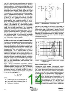
The total output offset voltage can be considerably reduced
by matching the source impedances looking out of the two
inputs. For example, one way to add bias current cancella-
tion to the circuit of Figure 1 is to insert a 12.1Ω series
resistor into the noninverting input from the 50Ω terminating
resistor. When the 50Ω source resistor is DC-coupled, this
increases the source impedance for the noninverting input
bias current to 37.1Ω. Since this is now equal to the imped-
ance looking out of the inverting input (RF || RG) for Figure 1,
the circuit cancels the gains for the bias currents to the
output, leaving only the offset current times the feedback
resistor as a residual DC error term at the output. Using the
750Ω feedback resistor, this output error is now less than
±0.85µA • 750Ω = ±640µV over the full temperature range for
the circuit of Figure 1, with a 12.1Ω resistor added as
described. The output DC offset is then dominated by the
input offset voltage multiplied by the signal gain. For the
circuit of Figure 1, this is a worst-case output DC offset of
±0.6mV • 20 = ±12mV over the full temperature range.
In this case, the input is brought into an inverting gain resistor
with the DC adjustment as an additional current summed into
the inverting node. The resistor values setting this offset
adjustment are much larger than the signal path resistors.
This ensures that this adjustment has minimal impact on the
loop gain and, hence, the frequency response.
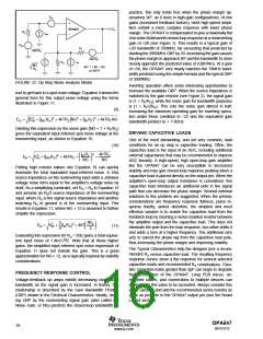
POWER SHUTDOWN OPERATION
The OPA847 provides an optional power shutdown feature
that can be used to reduce system power. If the VDIS control
pin is left unconnected, the OPA847 operates normally. This
shutdown is intended only as a power saving feature. For-
ward path isolation is very good for small signals. Large
signal isolation is not ensured. Using this feature to multiplex
two or more outputs together is not recommended. Large
signals applied to the shutdown output stages can turn on
parasitic devices, degrading signal linearity for the desired
channel.
Turn-on time is very quick from the shutdown condition,
typically < 60ns. Turn-off time is strongly dependent on the
external circuit configuration, but is typically 200ns for the
circuit of Figure 1. Using the OPA847 with higher external
resistor values, such has high-gain transimpedance circuits,
slows the shutdown time since the time constants for the
internal nodes to discharge are longer.
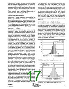
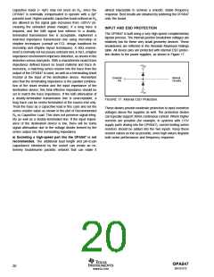
A fine-scale output offset null, or DC operating point adjust-
ment, is sometimes required. Numerous techniques are
available for introducing a DC offset control into an op amp
circuit. Most of these techniques eventually reduce to setting
up a DC current through the feedback resistor. One key
consideration to selecting a technique is to ensure that it has
a minimal impact on the desired signal path frequency
response. If the signal path is intended to be noninverting,
the offset control is best applied as an inverting summing
signal to avoid interaction with the signal source. If the signal
path is intended to be inverting, applying the offset control to
the noninverting input can be considered. For a DC-coupled
inverting input signal, this DC offset signal sets up a DC
current back into the source that must be considered. An
offset adjustment placed on the inverting op amp input can
also change the noise gain and frequency response flatness.
Figure 15 shows one example of an offset adjustment for a
DC-coupled signal path that has minimum impact on the
signal frequency response.
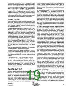
To shutdown, the control pin must be asserted low. This logic
control is referenced to the positive supply, as shown in the
simplified circuit of Figure 16.
+VS
8kΩ
Q1
+5V
VCC
Power-supply decoupling
not shown.
17kΩ
120kΩ
VO
OPA847
0.1µF
48Ω
IS
VDIS
Control
–VS
VEE
–5V
FIGURE 16. Simplified Shutdown Control Circuit.
+5V
RG
50Ω
RF
1kΩ
In normal operation, base current to Q1 is provided through
the 120kΩ resistor, while the emitter current through the 8kΩ
resistor sets up a voltage drop that is inadequate to turn on
the two diodes in Q1’s emitter. As VDIS is pulled low,
additional current is pulled through the 8kΩ resistor, even-
tually turning on these two diodes (≈ 180µA). At this point,
any further current pulled out of VDIS goes through those
diodes holding the emitter-base voltage of Q1 at approxi-
mately 0V. This shuts off the collector current out of Q1,
turning the amplifier off. The supply current in the shutdown
mode is only that required to operate the circuit of Figure 16.
VI
5kΩ
5kΩ
±200mV Output Adjustment
20kΩ
100Ω
0.1µF
V
RF
O = –
VI
= –20V/V
RG
–5V
FIGURE 15. DC-Coupled, Inverting Gain of –20 with Output
Offset Adjustment.
OPA847
18
SBOS251E
www.ti.com

 TI [ TEXAS INSTRUMENTS ]