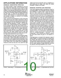
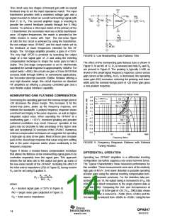
This circuit uses two stages of forward gain with an overall
feedback loop to set the input impedance match. The input
transformer provides both a noiseless voltage gain and a
signal inversion to retain an overall noninverting signal path
from PI to PO. The second amplifier stage is inverting to
provide the correct feedback polarity through the 6.19kΩ
resistor. To achieve a 50Ω input match at the primary of the
1:2 transformer, the secondary must see a 200Ω load imped-
ance. At higher frequencies, the match is provided by the
200Ω resistor in series with 10pF. The low-noise figure
(4.3dB) for this circuit is achieved by using the transformer,
the low-voltage noise OPA847, and the input match set by
the feedback at lower frequencies intended for this HF
design. The 1st-stage amplifier provides a gain of +15V/V.
The very high SFDR is provided by operating the output
stage at a low signal gain of –2 and using the inverting
compensation technique to shape the noise gain to hold it
stable. This 2nd-stage compensation is set to intentionally
bandlimit the overall response to approximately 100MHz. For
output loads > 400Ω, this circuit can give a 2-tone SFDR that
exceeds 90dB through 30MHz. In narrowband applications,
the 3rd-order intercept exceeds 55dBm. Besides offering a
very high dynamic range, this circuit improves on standard
HF amplifiers by offering a precisely controlled gain and a
very flexible output interface capability.
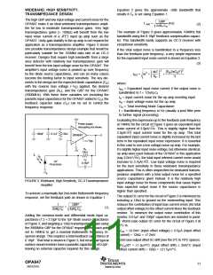
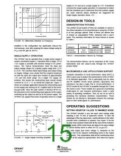
+5V
VI
VDIS
50Ω
50Ω
R1
50Ω
VO
OPA847
–5V
RF
750Ω
RG
66.5Ω
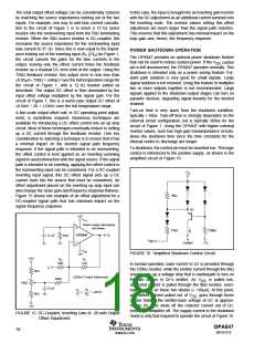
FIGURE 8. Low Noninverting Gain Flatness Trim.
The effect of this noninverting gain flatness tune is shown in
Figure 9. At an NG of 12, R1 is removed and only RF and RG
are present in Figure 8. The peaking is typically 4.5dB, as
shown in the small-signal frequency response curves versus
gain curves at this setting. As R1 is decreased, the operating
noise gain (NG) increases, reducing the peaking and band-
width until the nominal design point of +20 noise gain gives
a non-peaked response.
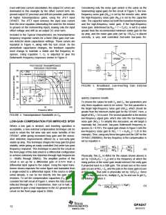
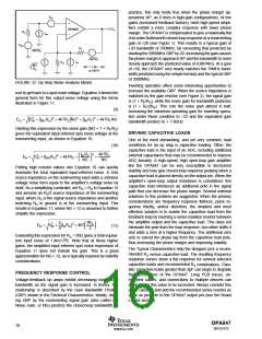
NONINVERTING GAIN FLATNESS TUNE
0.5
NONINVERTING GAIN FLATNESS COMPENSATION
V
O = 200mVPP
NG = 12
NG = 14
NG = 16
Decreasing the operating gain from the nominal design point of
+20 decreases the phase margin. This increases Q for the
closed-loop poles, peaks up the frequency response, and
extends the bandwidth. A peaked frequency response shows
overshoot and ringing in the pulse response, as well as higher
integrated output noise. When operating the OPA847 at a
noninverting gain < +12V/V, increased peaking and possible
sustained oscillations may result. However, operation at low
gains may be desirable to take advantage of the higher slew
rate and exceptional DC precision of the OPA847. Numerous
external compensation techniques are suggested for operating
a high-gain op amp at low gains. Most of these give zero/pole
pairs in the closed-loop response that cause long term settling
tails in the pulse response and/or phase nonlinearity in the
frequency response.
0.4
0.3
AV = +12V/V
NG = Noise Gain
0.2
0.1
0
–0.1
–0.2
–0.3
–0.4
–0.5
NG = 18
NG = 20
1
10
100
Frequency (MHz)
1000
FIGURE 9. Frequency Response Flatness with External
Tuning Resistor.
Figure 8 shows a resistor-based compensation technique
that allows the flatness at low noninverting signal gains to be
controlled separately from the signal gain. This approach
retains the full slew rate to the output but gives up some of
the low-noise benefit of the OPA847. Including the effect of
the total source impedance (25Ω in Figure 8), tuning resistor
R1 can be set using Equation 8.
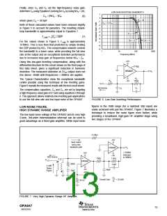
DIFFERENTIAL OPERATION
Operating two OPA847 amplifiers in a differential inverting
configuration can further suppress even-order harmonic terms.
The Typical Characteristics show measured performance for
this condition. These measurements were done at the relatively
high gain of 40V/V. Even lower distortion is possible operating
at lower gains using the external inverting compensation tech-
niques, as discussed previously. For the distortion data pre-
sented in Figure 10, the output swing is increased to 4VPP into
400Ω to allow direct comparison to the single-channel data at
2VPP into 200Ω. Comparing the 2nd- and 3rd-harmonics at
20MHz in Figure 10 to the gain of +20, 2VPP, 200Ω data, shows
the 2nd-harmonic is reduced to –76dBc (from –67dBc) and the
3rd-harmonic is reduced from –80dBc to –85dBc. Using the two
RF + RSAV
R1 =
(8)
NG − AV
where:
AV = desired signal gain (+12V/V in Figure 8)
NG = target noise gain (adjusted in Figure 9)
RS = total source impedance
OPA847
14
SBOS251E
www.ti.com

 TI [ TEXAS INSTRUMENTS ]