capacitive loads (< 4pF) may not need an RS, since the
OPA847 is nominally compensated to operate with a 2pF
parasitic load. Higher parasitic capacitive loads without an RS
are allowed as the signal gain increases from +20V/V (in-
creasing the unloaded phase margin). If a long trace is
required, and the 6dB signal loss intrinsic to a doubly-
terminated transmission line is acceptable, implement a
matched impedance transmission line using microstrip or
stripline techniques (consult an ECL design handbook for
microstrip and stripline layout techniques). A 50Ω environ-
ment is normally not necessary onboard and, in fact, a higher
impedance environment improves distortion, as shown in the
distortion versus load plots. With a characteristic board trace
impedance defined based on board material and trace di-
mensions, a matching series resistor into the trace from the
output of the OPA847 is used, as well as a terminating shunt
resistor at the input of the destination device. Remember
also that the terminating impedance is the parallel combina-
tion of the shunt resistor and the input impedance of the
destination device; this total effective impedance should be
set to match the trace impedance. If the 6dB attenuation of
a doubly-terminated transmission line is unacceptable, a
long trace can be series-terminated at the source-end only.
Treat the trace as a capacitive load in this case and set the
series resistor value as shown in the plot of Recommended
RS vs Capacitive Load. This does not preserve signal integ-
rity as well as a doubly-terminated line. If the input imped-
ance of the destination device is low, there will be some
signal attenuation due to the voltage divider formed by the
series output into the terminating impedance.
almost impossible to achieve a smooth, stable frequency
response. Best results are obtained by soldering the OPA847
onto the board.
INPUT AND ESD PROTECTION
The OPA847 is built using a very high-speed complementary
bipolar process. The internal junction breakdown voltages are
relatively low for these very small geometry devices. These
breakdowns are reflected in the Absolute Maximum Ratings
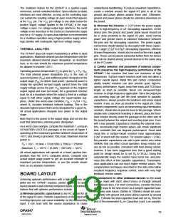
table. All device pins are protected with internal ESD protec-
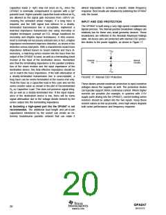
tion diodes to the power supplies, as shown in Figure 17.
+VCC
External
Pin
Internal
Circuitry
–VCC
FIGURE 17. Internal ESD Protection.
These diodes provide moderate protection to input overdrive
voltages above the supplies as well. The protection diodes
can typically support 30mA continuous current. Where higher
currents are possible (for example, in systems with ±15V
supply parts driving into the OPA847), current limiting series
resistors should be added into the two inputs. Keep these
resistor values as low as possible, since high values degrade
both noise performance and frequency response.
e) Socketing a high-speed part like the OPA847 is not
recommended. The additional lead length and pin-to-pin
capacitance introduced by the socket can create an ex-
tremely troublesome parasitic network that can make it
OPA847
20
SBOS251E
www.ti.com

 TI [ TEXAS INSTRUMENTS ]