supply of +5V and up to a single supply of +12V. If shutdown
is desired for single-supply operation, it is important to realize
that the shutdown pin is referenced from the positive supply
pin. Open collector (drain) interfaces are suggested for
single-supply operation above +5V.
–65
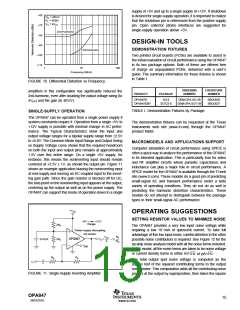
–75
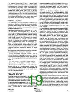
GD = 40V/V
L = 400Ω
O = 4VPP
R
V
2nd-Harmonic
–85
DESIGN-IN TOOLS
–95
DEMONSTRATION FIXTURES
3rd-Harmonic
–105
–115
Two printed circuit boards (PCBs) are available to assist in
the initial evaluation of circuit performance using the OPA847
in its two package options. Both of these are offered free
of charge as unpopulated PCBs, delivered with a user’s
guide. The summary information for these fixtures is shown
in Table I.
1
10
Frequency (MHz)
100
FIGURE 10. Differential Distortion vs Frequency.
ORDERING
NUMBER
LITERATURE
NUMBER
amplifiers in this configuration has significantly reduced the
2nd-harmonic, even after doubling the output voltage swing (to
4VPP) and the gain (to 40V/V).
PRODUCT
PACKAGE
OPA847ID
SO-8
DEM-OPA-SO-1B
DEM-OPA-SOT-1B
SBOU026
SBOU027
OPA847IDBV
SOT23-6
TABLE I. Demonstration Fixtures by Package.
SINGLE-SUPPLY OPERATION
The OPA847 can be operated from a single power supply if
system constraints require it. Operation from a single +5V to
+12V supply is possible with minimal change in AC perfor-
mance. The Typical Characteristics show the input and
output voltage ranges for a bipolar supply range from ±2.5V
to ±6.0V. The Common-Mode Input Range and Output Swing
vs Supply Voltage curve shows that the required headroom
on both the input and output pins remains at approximately
1.5V over this entire range. On a single +5V supply, for
instance, this means the noninverting input should remain
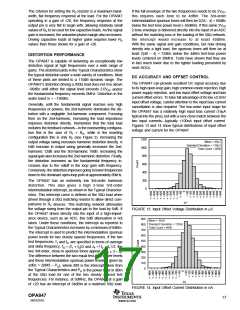
centered at +2.5V ± 1V, as should the output pin. Figure 11
shows an example application biasing the noninverting input
at mid-supply and running an AC-coupled input to the invert-
ing gain path. Since the gain resistor is blocked off for DC,
the bias point on the noninverting input appears at the output,
centering up the output as well as on the power supply. The
OPA847 can support this mode of operation down to a single
The demonstration fixtures can be requested at the Texas
Instruments web site (www.ti.com) through the OPA847
product folder.
MACROMODELS AND APPLICATIONS SUPPORT
Computer simulation of circuit performance using SPICE is
often a quick way to analyze the performance of the OPA847
in its intended application. This is particularly true for video
and RF amplifier circuits where parasitic capacitance and
inductance can play a major role in circuit performance. A
SPICE model for the OPA847 is available through the TI web
site (www.ti.com). These models do a good job of predicting
small-signal AC and transient performance under a wide
variety of operating conditions. They do not do as well in
predicting the harmonic distortion characteristics. These
models do not attempt to distinguish between the package
types in their small-signal AC performance.
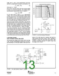
+VCC
OPERATING SUGGESTIONS
SETTING RESISTOR VALUES TO MINIMIZE NOISE
+5V
+12V
Range
2RF
2RF
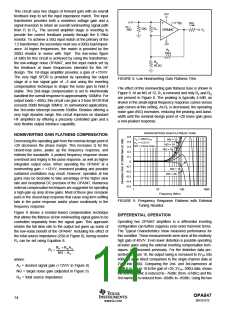
The OPA847 provides a very low input noise voltage while
requiring a low 18.1mA of quiescent current. To take full
advantage of this low input noise, careful attention to the other
possible noise contributors is required. See Figure 12 for the
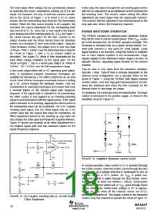
op amp noise analysis model with all the noise terms included.
In this model, all the noise terms are taken to be noise voltage
Power-supply decoupling
not shown.
VCC
RF
VO
=
OPA847
– VI
0.01µF
2
RG
VDIS
or current density terms in either nV/√Hz or pA/√Hz
.
RG
RF
The total output spot noise voltage is computed as the
square root of the squared contributing terms to the output
noise power. This computation adds all the contributing noise
powers at the output by superposition, then takes the square
VI
FIGURE 11. Single-Supply Inverting Amplifier.
OPA847
SBOS251E
15
www.ti.com

 TI [ TEXAS INSTRUMENTS ]