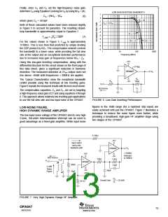
The criterion for setting the RS resistor is a maximum band-
width, flat frequency response at the load. For the OPA847
operating in a gain of +20, the frequency response at the
output pin is very flat to begin with, allowing relatively small
values of RS to be used for low capacitive loads. As the signal
gain is increased, the unloaded phase margin also increases.
Driving capacitive loads at higher gains requires lower RS
values than those shown for a gain of +20.
If the full envelope of the two frequencies needs to be 2VPP,
this requires each tone to be 4dBm. The 3rd-order
intermodulation spurious tones will then be 2(34 – 4) = 60dBc
below the test-tone power level (–56dBm). If this same 2VPP
2-tone envelope is delivered directly into the input of an ADC
without the matching loss or the loading of the 50Ω network,
the intercept would increase to at least 40dBm.
With the same signal and gain conditions, but now driving
directly into a light load, the spurious tones will then be at
least 2(40 – 4) = 72dBc below the 4dBm test-tone power
levels centered on 30MHz. Tests have shown that they are
in fact much lower due to the lighter loading presented by
most ADCs.
DISTORTION PERFORMANCE
The OPA847 is capable of delivering an exceptionally low
distortion signal at high frequencies over a wide range of
gains. The distortion plots in the Typical Characteristics show
the typical distortion under a wide variety of conditions. Most
of these plots are limited to a 110dB dynamic range. The
OPA847’s distortion driving a 200Ω load does not rise above
–90dBc until either the signal level exceeds 2.0VPP and/or
the fundamental frequency exceeds 5MHz. Distortion in the
audio band is < –130dBc.
DC ACCURACY AND OFFSET CONTROL
The OPA847 can provide excellent DC signal accuracy due
to its high open-loop gain, high common-mode rejection, high
power-supply rejection, and low input offset voltage and bias
current offset errors. To take full advantage of its low ±0.5mV
input offset voltage, careful attention to the input bias current
cancellation is also required. The low-noise input stage for
the OPA847 has a relatively high input bias current (19µA
typical into the pins), but with a very close match between the
two input currents—typically ±100nA input offset current.
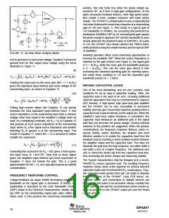
Figures 13 and 14 show typical distributions of input offset
voltage and current for the OPA847.
Generally, until the fundamental signal reaches very high
frequencies or powers, the 2nd-harmonic dominates the dis-
tortion with a negligible 3rd-harmonic component. Focusing
then on the 2nd-harmonic, increasing the load impedance
improves distortion directly. Remember that the total load
includes the feedback network—in the noninverting configura-
tion this is the sum of RF + RG, while in the inverting
configuration this is only RF (see Figure 2). Increasing the
output voltage swing increases harmonic distortion directly. A
6dB increase in output swing generally increases the 2nd-
harmonic 12dB and the 3rd-harmonic 18dB. Increasing the
signal gain also increases the 2nd-harmonic distortion. Finally,
the distortion increases as the fundamental frequency in-
creases due to the rolloff in the loop gain with frequency.
Conversely, the distortion improves going to lower frequencies
down to the dominant open-loop pole at approximately 80kHz.
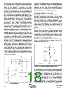
1200
Mean = 48µV
Standard Deviation = 110µV
1000
Total Count = 4040
800
600
400
200
0
The OPA847 has an extremely low 3rd-order harmonic
distortion. This also gives a high 2-tone 3rd-order
intermodulation intercept, as shown in the Typical Character-
istics. This intercept curve is defined at the 50Ω load when
driven through a 50Ω matching resistor to allow direct com-
parisons to RF devices. This matching network attenuates
the voltage swing from the output pin to the load by 6dB. If
the OPA847 drives directly into the input of a high-imped-
ance device, such as an ADC, this 6dB attenuation is not
taken. Under these conditions, the intercept as reported in
the Typical Characteristics increases by a minimum of 6dBm.
The intercept is used to predict the intermodulation spurious
power levels for two closely spaced frequencies. If the two
test frequencies, f1 and f2, are specified in terms of average
and delta frequency, fO = (f1 + f2)/2 and ∆f = f2 – f1 /2, the
two 3rd-order, close-in spurious tones appear at fO ± 3 • ∆f.
The difference between the two equal test-tone power levels
and these intermodulation spurious power levels is given by
∆dBc = 2(IM3 – PO), where IM3 is the intercept taken from
the Typical Characteristics and PO is the power level in dBm
at the 50Ω load for one of the two closely spaced test
frequencies. For instance, at 30MHz, the OPA847 at a gain
of +20 has an intercept of 34dBm at a matched 50Ω load.
µV
FIGURE 13. Input Offset Voltage Distribution in µV.
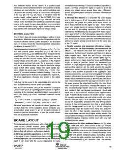
900
Mean = 50nA
Standard Deviation = 120nA
Total Count = 4040
800
700
600
500
400
300
200
100
0
nA
FIGURE 14. Input Offset Current Distribution in nA.
OPA847
SBOS251E
17
www.ti.com

 TI [ TEXAS INSTRUMENTS ]