Even with bias current cancellation, the output DC errors are
dominated in this example by the offset current term. Im-
proved output DC precision and drift are possible, particularly
at higher transimpedance gains, using the JFET input
OPA657. The JFET input removes the input bias current
from the error equation (eliminating the need for the resistor
to ground on the noninverting input), leaving only the input
offset voltage and drift as an output DC error term.
Considering only the noise gain (which is the same as the
noninverting signal gain) for the circuit of Figure 5, the low-
frequency noise gain (NG1) is set by the resistor ratio, while
the high-frequency noise gain (NG2) is set by the capacitor
ratio. The capacitor values set both the transition frequencies
and the high-frequency noise gain. If the high-frequency
noise gain, determined by NG2 = 1 + CS/CF, is set to a value
greater than the recommended minimum stable gain for the
op amp, and the noise gain pole (set by 1/RFCF) is placed
correctly, a very well controlled 2nd-order low-pass fre-
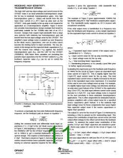
Included in the Typical Characteristics are transimpedance
frequency response curves for a fixed 20kΩ gain over vari-
ous detector diode capacitance settings. These curves are
repeated in Figure 4, along with the test circuit. As the
photodiode capacitance changes, the feedback capacitor
must change to maintain a stable and flat frequency re-
sponse. Using Equation 1, CF is adjusted to give the
Butterworth frequency responses shown in Figure 4.
+5V
VDIS
VO
OPA847
RG
200Ω
RF
850Ω
PHOTODIODE TRANSIMPEDANCE
FREQUENCY RESPONSE
VI
89
RF = 20kΩ
CD = 10pF
CS
39pF
CF
1.7pF
CF Adjusted
[20 log(20kΩ)]
86
83
80
77
74
71
CD = 20pF
CD = 50pF
–5V
CD = 100pF
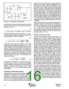
FIGURE 5. Broadband, Low-Inverting Gain External
Compensation.
VO
0.01µF
OPA847
20kΩ
20kΩ
IO
quency response results.
CF
CD
To choose the values for both CS and CF, two parameters and
only three equations need to be solved. The first parameter is
the target high-frequency noise gain (NG2), which should be
greater than the minimum stable gain for the OPA847. Here, a
target of NG2 = 24 is used. The second parameter is the desired
low-frequency signal gain, which also sets the low-frequency
noise gain (NG1). To simplify this discussion, we will target a
maximally flat, 2nd-order, low-pass Butterworth frequency re-
sponse (Q = 0.707). The signal gain shown in Figure 5 sets the
low-frequency noise gain to NG1 = 1 + RF/RG (= 5.25 in this
example). Then, using only these two gains and the GBP for the
OPA847 (3900MHz), the key frequency in the compensation is
set by Equation 4.
1
10
Frequency (MHz)
100
FIGURE 4. Transimpedance Bandwidth vs CD.
LOW-GAIN COMPENSATION FOR IMPROVED SFDR
Where a low gain is desired, and inverting operation is
acceptable, a new external compensation technique can be
used to retain the full slew rate and noise benefits of the
OPA847, while giving increased loop gain and the associ-
ated distortion improvements offered by a non-unity-gain
stable op amp. This technique shapes the loop gain for good
stability, while giving an easily controlled 2nd-order low-pass
frequency response. This technique is used for the circuit on
the front page of this data sheet in a differential configuration
to achieve extremely low distortion through high frequencies
(< –90dBc through 30MHz). The amplifier portion of this
circuit is set up for a differential gain of 8.5V/V from a
differential input signal to the output. Using the input trans-
former shown improves the noise figure and translates from
a single-ended to a differential signal. If the source is differ-
ential already, it can be fed directly into the gain setting
resistors. To set the compensation capacitors (CS and CF),
consider the half circuit of Figure 5, where the 50Ω source is
reflected through the 1:2 transformer, then cut in half, and
grounded to give a total impedance to the AC ground for the
circuit on the front page equal to 200Ω.
GBP
NG21
NG1
NG2
NG1
NG2
ZO
=
1−
− 1− 2
(4)
Physically, this ZO (4.4MHz for the values shown above) is
set by 1/(2πRF(CF + CS)) and is the frequency at which the
rising portion of the noise gain would intersect the unity gain
if projected back to a 0dB gain. The actual zero in the noise
gain occurs at NG1 • ZO and the pole in the noise gain occurs
at NG2 • ZO. That pole is physically set by 1/(RFCF). Since
GBP is expressed in Hz, multiply ZO by 2π and use to get CF
by solving Equation 5.
1
CF
=
= 1.76pF
(
)
(5)
2πRFZONG2
OPA847
12
SBOS251E
www.ti.com

 TI [ TEXAS INSTRUMENTS ]