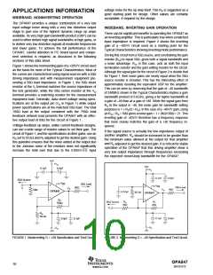
WIDEBAND, HIGH SENSITIVITY,
TRANSIMPEDANCE DESIGN
Equation 2 gives the approximate –3dB bandwidth that
results if CF is set using Equation 1.
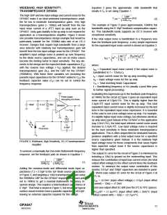
The high GBP and low input voltage and current noise for the
OPA847 make it an ideal wideband transimpedance ampli-
fier for low to moderate transimpedance gains. Very high
transimpedance gains (> 100kΩ) will benefit from the low
input noise current of a JFET input op amp such as the
OPA657. Unity-gain stability in the op amp is not required for
application as a transimpedance amplifier. Figure 3 shows
one possible transimpedance design example that would be
particularly suitable for the 155Mbit data rate of an OC-3
receiver. Designs that require high bandwidth from a large
area detector with relatively low transimpedance gain will
benefit from the low input voltage noise for the OPA847. The
amplifier’s input voltage noise is peaked up over frequency
by the diode source capacitance, and can (in many cases)
become the limiting factor to input sensitivity. The key ele-
ments to the design are the expected diode capacitance (CD)
with the reverse bias voltage (–VB) applied, the desired
transimpedance gain (RF), and the GBP for the OPA847
(3900MHz). With these three variables set (including the
parasitic input capacitance for the OPA847 added to CD), the
feedback capacitor value (CF) can be set to control the
frequency response.
GBP
f−3dB
=
Hz
(
)
(2)
2πRF CD
The example of Figure 3 gives approximately 104MHz flat
bandwidth using the 0.18pF feedback compensation capaci-
tor. This bandwidth easily supports an OC-3 receiver with
exceptional sensitivity.
If the total output noise is bandlimited to a frequency less
than the feedback pole frequency, a very simple expression
for the equivalent input noise current is shown as Equation 3.
(3)
2
2
E 2πC F
(
)
4kT
RF
N
D
2
iEQ
=
iN
+
+
3
where:
iEQ = Equivalent input noise current if the output noise is
bandlimited to f < 1/2πRFCF
iN = Input current noise for the op amp inverting input
eN = Input voltage noise for the op amp
CD = Total Inverting Node Capacitance
f = Bandlimiting frequency in Hz (usually a post filter prior
to further signal processing)
+5V
Evaluating this expression up to the feedback pole frequency
at 74MHz for the circuit of Figure 3 gives an equivalent input
noise current of 3.0pA/√Hz. This is slightly higher than the
2.5pA/√Hz input current noise for the op amp. This total
equivalent input current noise is slightly increased by the last
term in the equivalent input noise expression. It is essential
in this case to use a low-voltage noise op amp. For example,
if a slightly higher input noise voltage, but otherwise identical,
op amp were used instead of the OPA847 in this application
(say 2.0nV/√Hz), the total input referred current noise would
increase to 3.7pA/√Hz. Low input voltage noise is required
for the best sensitivity in these wideband transimpedance
applications. This is often unspecified for dedicated transim-
pedance amplifiers with a total output noise for a specified
source capacitance given instead. It is the relatively high
input voltage noise for those components that cause higher
than expected output noise if the source capacitance is
higher than specified.
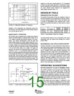
Power-supply
decoupling not shown.
100pF
0.1µF
12kΩ
OPA847
VDIS
RF
12kΩ
–5V
λ
CF
1pF
Photodiode
0.18pF
–VB
FIGURE 3. Wideband, High Sensitivity, OC-3 Transimpedance
Amplifier.
To achieve a maximally flat 2nd-order Butterworth frequency
response, set the feedback pole as shown in Equation 1.
The output DC error for the circuit of Figure 3 is minimized by
including a 12kΩ to ground on the noninverting input. This
reduces the contribution of input bias current errors (for total
output offset voltage) to the offset current times the feedback
resistor. To minimize the output noise contribution of this
resistor, 0.01µF and 100pF capacitors are included in paral-
lel. Worst-case output DC error for the circuit of Figure 3 at
25°C is:
1
GBP
=
(1)
2πRFCF
4πRFCD
Adding the common-mode and differential mode input ca-
pacitance (1.2 + 2.5)pF to the 1pF diode source capacitance
of Figure 3, and targeting a 12kΩ transimpedance gain using
the 3900MHz GBP for the OPA847 requires a feedback pole
set to 74MHz to get a nominal Butterworth frequency re-
sponse design. This requires a total feedback capacitance of
0.18pF. That total is shown in Figure 3, but recall that typical
surface-mount resistors have a parasitic capacitance of 0.2pF,
leaving no external capacitor required for this design.
VOS = ±0.5mV (input offset voltage) ± 0.6µA (input offset
current) • 12kΩ = ±7.2mV
Worst-case output offset DC drift (over the 0°C to 70°C span) is:
dVOS/dT = ±1.5µV/°C (input offset drift) ± 2nA/°C (input
offset current drift) • 12kΩ = ±21.5µV/°C.
OPA847
SBOS251E
11
www.ti.com

 TI [ TEXAS INSTRUMENTS ]