voltage noise for the op amp itself. This RG is suggested as a
good starting point for design. Other values are certainly
acceptable, if required by the design.
APPLICATIONS INFORMATION
WIDEBAND, NONINVERTING OPERATION
The OPA847 provides a unique combination of a very low
input voltage noise along with a very low distortion output
stage to give one of the highest dynamic range op amps
available. Its very high gain bandwidth product (GBP) can be
used to either deliver high signal bandwidths at high gains, or
to deliver very low distortion signals at moderate frequencies
and lower gains. To achieve the full performance of the
OPA847, careful attention to PC board layout and compo-
nent selection is required, as discussed in the following
sections of this data sheet.
WIDEBAND, INVERTING GAIN OPERATION
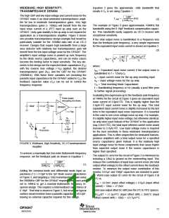
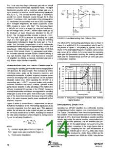
There can be significant benefits to operating the OPA847 as
an inverting amplifier. This is particularly true when a matched
input impedance is required. Figure 2 shows the inverting
gain of a –40V/V circuit used as a starting point for the
Typical Characteristics showing inverting mode performance.
Driving this circuit from a 50Ω source, and constraining the gain
resistor (RG) to equal 50Ω, gives both a signal bandwidth and
a noise advantage. RG, in this case, acts as both the input
termination resistor and the gain setting resistor for the circuit.
Although the signal gain for the circuit of Figure 2 is double that
for Figure 1, their noise gains are nearly equal when the 50Ω
source resistor is included. This has the interesting effect of
approximately doubling the equivalent GBP for the amplifier.
This can be seen by observing that the gain of –40 bandwidth
of 240MHz shown in the Typical Characteristics implies a gain
bandwidth product of 9.6GHz, giving a far higher bandwidth at
a gain of –40 than at a gain of +40. While the signal gain from
RG to the output is –40, the noise gain for bandwidth setting
purposes is 1 + RF/(2 • RG). In the case of a –40V/V gain, using
an RG = RS = 50Ω gives a noise gain = 1 + 2kΩ/100Ω = 21. This
inverting gain of –40V/V therefore has a frequency response
that more closely matches the gain of a +20 frequency re-
sponse.
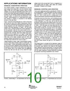
Figure 1 shows the noninverting gain of a +20V/V circuit used
as the basis for most of the Typical Characteristics. Most of
the curves are characterized using signal sources with a 50Ω
driving impedance and with measurement equipment pre-
senting a 50Ω load impedance. In Figure 1, the 50Ω shunt
resistor at the VI terminal matches the source impedance of
the test generator, while the 50Ω series resistor at the VO
terminal provides a matching resistor for the measurement
equipment load. Generally, data sheet voltage swing speci-
fications are at the output pin (VO in Figure 1) while output
power specifications are at the matched 50Ω load. The total
100Ω load at the output combined with the 790Ω total
feedback network load presents the OPA847 with an effec-
tive output load of 89Ω for the circuit of Figure 1.
Voltage-feedback op amps, unlike current-feedback designs,
can use a wide range of resistor values to set their gain. The
circuit of Figure 1, and the specifications at other gains, use an
RG set to 39.2Ω and RF adjusted to get the desired gain. Using
this guideline ensures that the noise added at the output due
to the Johnson noise of the resistors does not significantly
increase the total over that due to the 0.85nV/√Hz input
If the signal source is actually the low impedance output of
another amplifier, RG should be increased to be greater than
the minimum value allowed at the output for that amplifier
and RF adjusted to get the desired gain. It is critical for stable
operation of the OPA847 that this driving amplifier show a
very low output impedance through frequencies exceeding
the expected closed-loop bandwidth for the OPA847.
+5V
+VS
+5V
+VS
0.1µF
6.8µF
+
+
0.1µF
6.8µF
50Ω Source
VDIS
50Ω Load
VDIS
50Ω Load
50Ω
VI
VO
VO
50Ω
50Ω
OPA847
0.01µF
95.3Ω
OPA847
RF
750Ω
RG
50Ω
RF
2kΩ
50Ω Source
VI
RG
39.2Ω
0.1µF
6.8µF
6.8µF
0.1µF
+
+
–VS
–5V
–VS
–5V
FIGURE 1. Noninverting G = +20 Specification and Test Circuit.
FIGURE 2. Noninverting G = –40 Specification and Test Circuit.
OPA847
10
SBOS251E
www.ti.com

 TI [ TEXAS INSTRUMENTS ]