OMAP-L137 Low-Power Applications Processor
www.ti.com
SPRS563A–SEPTEMBER 2008–REVISED OCTOBER 2008
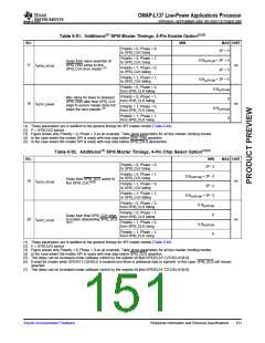
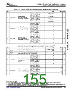
Table 6-57. General Timing Requirements for SPI1 Master Modes (continued)
NO.
MIN
MAX UNIT
Polarity = 0, Phase = 0,
from SPI1_CLK falling
0.5tc(SPC)M -3
Polarity = 0, Phase = 1,
from SPI1_CLK rising
0.5tc(SPC)M -3
Output hold time,
SPI1_SIMO valid after
receive edge of SPI1_CLK
6
7
8
toh(SPC_SIMO)M
ns
Polarity = 1, Phase = 0,
from SPI1_CLK rising
0.5tc(SPC)M -3
Polarity = 1, Phase = 1,
from SPI1_CLK falling
0.5tc(SPC)M -3
Polarity = 0, Phase = 0,
to SPI1_CLK falling
0
0
0
0
5
5
5
5
Polarity = 0, Phase = 1,
to SPI1_CLK rising
Input Setup Time,
SPI1_SOMI valid before
receive edge of SPI1_CLK
tsu(SOMI_SPC)M
ns
Polarity = 1, Phase = 0,
to SPI1_CLK rising
Polarity = 1, Phase = 1,
to SPI1_CLK falling
Polarity = 0, Phase = 0,
from SPI1_CLK falling
Polarity = 0, Phase = 1,
from SPI1_CLK rising
Input Hold Time,
SPI1_SOMI valid after
receive edge of SPI1_CLK
tih(SPC_SOMI)M
ns
Polarity = 1, Phase = 0,
from SPI1_CLK rising
Polarity = 1, Phase = 1,
from SPI1_CLK falling
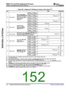
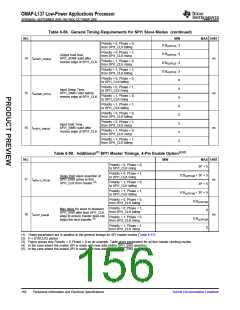
Table 6-58. General Timing Requirements for SPI1 Slave Modes(1)
NO.
MIN
MAX UNIT
greater of 2P or
9
tc(SPC)S
Cycle Time, SPI1_CLK, All Slave Modes
20 ns
256P ns
10 tw(SPCH)S
11 tw(SPCL)S
Pulse Width High, SPI1_CLK, All Slave Modes
Pulse Width Low, SPI1_CLK, All Slave Modes
10
10
ns
ns
Polarity = 0, Phase = 0,
to SPI1_CLK rising
2P
2P
2P
2P
Polarity = 0, Phase = 1,
to SPI1_CLK rising
Setup time, transmit data
written to SPI before initial
clock edge from
12 tsu(SOMI_SPC)S
ns
Polarity = 1, Phase = 0,
to SPI1_CLK falling
master.(2)(3)
Polarity = 1, Phase = 1,
to SPI1_CLK falling
Polarity = 0, Phase = 0,
from SPI1_CLK rising
9.7
Polarity = 0, Phase = 1,
from SPI1_CLK falling
9.7
ns
Delay, subsequent bits
valid on SPI1_SOMI after
transmit edge of SPI1_CLK
13 td(SPC_SOMI)S
Polarity = 1, Phase = 0,
from SPI1_CLK falling
9.7
Polarity = 1, Phase = 1,
from SPI1_CLK rising
9.7
(1) P = SYSCLK2 period
(2) First bit may be MSB or LSB depending upon SPI configuration. SO(0) refers to first bit and SO(n) refers to last bit output on
SPI1_SOMI. SI(0) refers to the first bit input and SI(n) refers to the last bit input on SPI1_SIMO.
(3) Measured from the termination of the write of new data to the SPI module, In analyzing throughput requirements, additional internal bus
cycles must be accounted for to allow data to be written to the SPI module by the DSP CPU.
Submit Documentation Feedback
Peripheral Information and Electrical Specifications
155

 TI [ TEXAS INSTRUMENTS ]