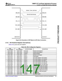
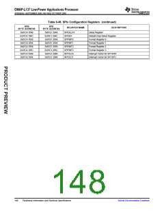
OMAP-L137 Low-Power Applications Processor
www.ti.com
SPRS563A–SEPTEMBER 2008–REVISED OCTOBER 2008
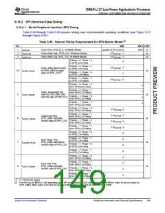
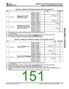
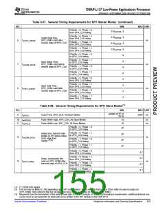
Table 6-51. Additional(1) SPI0 Master Timings, 4-Pin Enable Option(2)(3)
NO.
MIN
MAX UNIT
3P + 5
Polarity = 0, Phase = 0,
to SPI0_CLK rising
Polarity = 0, Phase = 1,
to SPI0_CLK rising
0.5tc(SPC)M + 3P + 5
Delay from slave assertion of
SPI0_ENA active to first
SPI0_CLK from master.(4)
17 td(ENA_SPC)M
ns
Polarity = 1, Phase = 0,
to SPI0_CLK falling
3P + 5
Polarity = 1, Phase = 1,
to SPI0_CLK falling
0.5tc(SPC)M + 3P + 5
Polarity = 0, Phase = 0,
from SPI0_CLK falling
0.5tc(SPC)M
Polarity = 0, Phase = 1,
from SPI0_CLK falling
Max delay for slave to deassert
SPI0_ENA after final SPI0_CLK
edge to ensure master does not
begin the next transfer.(5)
0
0.5tc(SPC)M
0
18 td(SPC_ENA)M
ns
Polarity = 1, Phase = 0,
from SPI0_CLK rising
Polarity = 1, Phase = 1,
from SPI0_CLK rising
(1) These parameters are in addition to the general timings for SPI master modes (Table 6-49).
(2) P = SYSCLK2 period
(3) Figure shows only Polarity = 0, Phase = 0 as an example. Table gives parameters for all four master clocking modes.
(4) In the case where the master SPI is ready with new data before SPI0_ENA assertion.
(5) In the case where the master SPI is ready with new data before SPI0_EN A deassertion.
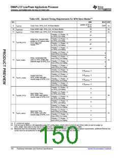
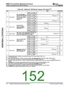
Table 6-52. Additional(1) SPI0 Master Timings, 4-Pin Chip Select Option(2)(3)
NO.
MIN
MAX UNIT
Polarity = 0, Phase = 0,
to SPI0_CLK rising
2P -3
Polarity = 0, Phase = 1,
to SPI0_CLK rising
0.5tc(SPC)M + 2P -3
Delay from SPI0_SCS active to
first SPI0_CLK(4)(5)
19 td(SCS_SPC)M
ns
Polarity = 1, Phase = 0,
to SPI0_CLK falling
2P -3
Polarity = 1, Phase = 1,
to SPI0_CLK falling
0.5tc(SPC)M + 2P -3
Polarity = 0, Phase = 0,
from SPI0_CLK falling
0.5tc(SPC)M
Polarity = 0, Phase = 1,
from SPI0_CLK falling
0
0.5tc(SPC)M
0
Delay from final SPI0_CLK edge
20 td(SPC_SCS)M
to master deasserting SPI0_SCS
ns
(6)(7)
Polarity = 1, Phase = 0,
from SPI0_CLK rising
Polarity = 1, Phase = 1,
from SPI0_CLK rising
(1) These parameters are in addition to the general timings for SPI master modes (Table 6-49).
(2) P = SYSCLK2 period
(3) Figure shows only Polarity = 0, Phase = 0 as an example. Table gives parameters for all four master clocking modes.
(4) In the case where the master SPI is ready with new data before SPI0_SCS assertion.
(5) This delay can be increased under software control by the register bit field SPIDELAY.C2TDELAY[4:0].
(6) Except for modes when SPIDAT1.CSHOLD is enabled and there is additional data to transmit. In this case, SPI0_SCS will remain
asserted.
(7) This delay can be increased under software control by the register bit field SPIDELAY.T2CDELAY[4:0].
Submit Documentation Feedback
Peripheral Information and Electrical Specifications
151

 TI [ TEXAS INSTRUMENTS ]