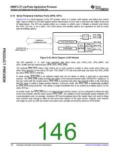
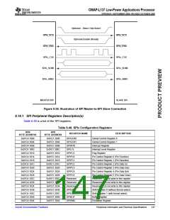
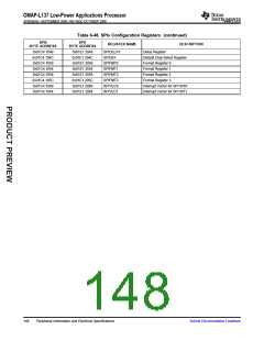
OMAP-L137 Low-Power Applications Processor
www.ti.com
SPRS563A–SEPTEMBER 2008–REVISED OCTOBER 2008
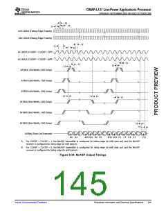
6.16.2 SPI Electrical Data/Timing
6.16.2.1 Serial Peripheral Interface (SPI) Timing
Table 6-49 through Table 6-64 assume testing over recommended operating conditions (see Figure 6-37
through Figure 6-40).
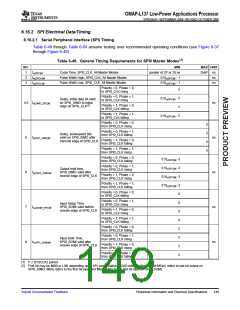
Table 6-49. General Timing Requirements for SPI0 Master Modes(1)
NO.
1
MIN
greater of 2P or 20 ns
0.5tc(SPC)M - 1
MAX UNIT
tc(SPC)M
Cycle Time, SPI0_CLK, All Master Modes
Pulse Width High, SPI0_CLK, All Master Modes
Pulse Width Low, SPI0_CLK, All Master Modes
256P ns
2
tw(SPCH)M
tw(SPCL)M
ns
ns
3
0.5tc(SPC)M - 1
Polarity = 0, Phase = 0,
to SPI0_CLK rising
5
0.5tc(SPC)M - 5
5
Polarity = 0, Phase = 1,
Delay, initial data bit valid
to SPI0_CLK rising
4,5 td(SIMO_SPC)M
on SPI0_SIMO to initial
ns
edge on SPI0_CLK(2)
Polarity = 1, Phase = 0,
to SPI0_CLK falling
Polarity = 1, Phase = 1,
to SPI0_CLK falling
0.5tc(SPC)M - 5
Polarity = 0, Phase = 0,
from SPI0_CLK rising
5
Polarity = 0, Phase = 1,
5
Delay, subsequent bits
from SPI0_CLK falling
5
6
7
8
td(SPC_SIMO)M
toh(SPC_SIMO)M
tsu(SOMI_SPC)M
tih(SPC_SOMI)M
valid on SPI0_SIMO after
ns
5
Polarity = 1, Phase = 0,
from SPI0_CLK falling
transmit edge of SPI0_CLK
Polarity = 1, Phase = 1,
from SPI0_CLK rising
5
Polarity = 0, Phase = 0,
from SPI0_CLK falling
0.5tc(SPC)M -3
Polarity = 0, Phase = 1,
from SPI0_CLK rising
0.5tc(SPC)M -3
Output hold time,
SPI0_SIMO valid after
receive edge of SPI0_CLK
ns
Polarity = 1, Phase = 0,
from SPI0_CLK rising
0.5tc(SPC)M -3
Polarity = 1, Phase = 1,
from SPI0_CLK falling
0.5tc(SPC)M -3
Polarity = 0, Phase = 0,
to SPI0_CLK falling
0
0
0
0
5
5
5
5
Polarity = 0, Phase = 1,
Input Setup Time,
to SPI0_CLK rising
SPI0_SOMI valid before
receive edge of SPI0_CLK
ns
Polarity = 1, Phase = 0,
to SPI0_CLK rising
Polarity = 1, Phase = 1,
to SPI0_CLK falling
Polarity = 0, Phase = 0,
from SPI0_CLK falling
Polarity = 0, Phase = 1,
from SPI0_CLK rising
Input Hold Time,
SPI0_SOMI valid after
receive edge of SPI0_CLK
ns
Polarity = 1, Phase = 0,
from SPI0_CLK rising
Polarity = 1, Phase = 1,
from SPI0_CLK falling
(1) P = SYSCLK2 period
(2) First bit may be MSB or LSB depending upon SPI configuration. MO(0) refers to first bit and MO(n) refers to last bit output on
SPI0_SIMO. MI(0) refers to the first bit input and MI(n) refers to the last bit input on SPI0_SOMI.
Submit Documentation Feedback
Peripheral Information and Electrical Specifications
149

 TI [ TEXAS INSTRUMENTS ]