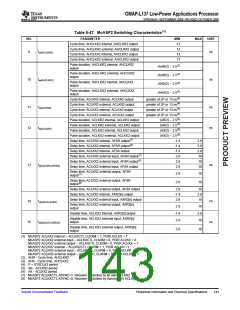
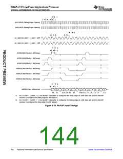
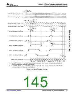
OMAP-L137 Low-Power Applications Processor
www.ti.com
SPRS563A–SEPTEMBER 2008–REVISED OCTOBER 2008
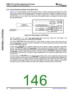
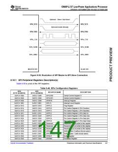
Optional − Slave Chip Select
SPIx_SCS
SPIx_ENA
SPIx_CLK
SPIx_SOMI
SPIx_SIMO
SPIx_SCS
SPIx_ENA
SPIx_CLK
SPIx_SOMI
SPIx_SIMO
Optional Enable (Ready)
MASTER SPI
SLAVE SPI
Figure 6-36. Illustration of SPI Master-to-SPI Slave Connection
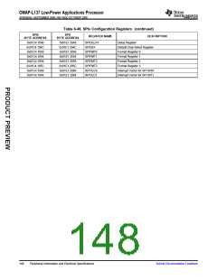
6.16.1 SPI Peripheral Registers Description(s)
Table 6-48 is a list of the SPI registers.
Table 6-48. SPIx Configuration Registers
SPI0
BYTE ADDRESS
SPI1
REGISTER NAME
DESCRIPTION
BYTE ADDRESS
0x01E1 2000
0x01E1 2004
0x01E1 2008
0x01E1 200C
0x01E1 2010
0x01E1 2014
0x01E1 2018
0x01E1 201C
0x01E1 2020
0x01E1 2024
0x01E1 2028
0x01E1 202C
0x01E1 2030
0x01E1 2034
0x01E1 2038
0x01E1 203C
0x01E1 2040
0x01E1 2044
0x01C4 1000
0x01C4 1004
0x01C4 1008
0x01C4 100C
0x01C4 1010
0x01C4 1014
0x01C4 1018
0x01C4 101C
0x01C4 1020
0x01C4 1024
0x01C4 1028
0x01C4 102C
0x01C4 1030
0x01C4 1034
0x01C4 1038
0x01C4 103C
0x01C4 1040
0x01C4 1044
SPIGCR0
SPIGCR1
SPIINT0
SPILVL
Global Control Register 0
Global Control Register 1
Interrupt Register
Interrupt Level Register
SPIFLG
SPIPC0
SPIPC1
SPIPC2
SPIPC3
SPIPC4
SPIPC5
Reserved
Reserved
Reserved
SPIDAT0
SPIDAT1
SPIBUF
SPIEMU
Flag Register
Pin Control Register 0 (Pin Function)
Pin Control Register 1 (Pin Direction)
Pin Control Register 2 (Pin Data In)
Pin Control Register 3 (Pin Data Out)
Pin Control Register 4 (Pin Data Set)
Pin Control Register 5 (Pin Data Clear)
Reserved - Do not write to this register
Reserved - Do not write to this register
Reserved - Do not write to this register
Shift Register 0 (without format select)
Shift Register 1 (with format select)
Buffer Register
Emulation Register
Submit Documentation Feedback
Peripheral Information and Electrical Specifications
147

 TI [ TEXAS INSTRUMENTS ]