LM5116
www.ti.com
SNVS499G –FEBRUARY 2007–REVISED MARCH 2013
be used to discharge CFT in the event of an input under-voltage condition.
RUV1 x RUV2
RUV1 + RUV2
1.215 x (RUV1 + RUV2
VIN x RUV1
)
x CFT x ln
tOFF = -
1 -
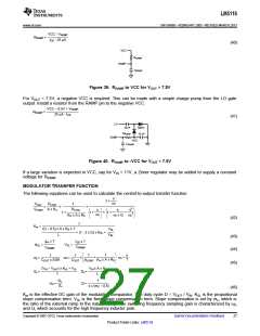
If under-voltage shutdown is not required, RUV1 and RUV2 can be eliminated and the off-time becomes:
1.215V
tOFF = CFT
x
5 mA
(25)
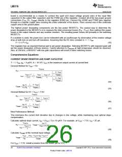
The voltage at the UVLO pin should never exceed 16V when using an external set-point divider. It may be
necessary to clamp the UVLO pin at high input voltages. For the design example, RUV2 = 102 kΩ and RUV1 = 21
kΩ for a shut-down voltage of 6.6V. If sustained short circuit protection is required, CFT ≥ 1 µF will limit the short
circuit power dissipation. D2 may be installed when using CFT with RUV1 and RUV2
.
MOSFETs
Selection of the power MOSFETs is governed by the same tradeoffs as switching frequency. Breaking down the
losses in the high-side and low-side MOSFETs is one way to determine relative efficiencies between different
devices. When using discrete SO-8 MOSFETs the LM5116 is most efficient for output currents of 2A to 10A.
Losses in the power MOSFETs can be broken down into conduction loss, gate charging loss, and switching loss.
Conduction, or I2R loss PDC, is approximately:
PDC(HO-MOSFET) = D x (IO2 x RDS(ON) x 1.3)
PDC(LO-MOSFET) = (1 - D) x (IO2 x RDS(ON) x 1.3)
(26)
(27)
Where D is the duty cycle. The factor 1.3 accounts for the increase in MOSFET on-resistance due to heating.
Alternatively, the factor of 1.3 can be ignored and the on-resistance of the MOSFET can be estimated using the
RDS(ON) vs Temperature curves in the MOSFET datasheet. Gate charging loss, PGC, results from the current
driving the gate capacitance of the power MOSFETs and is approximated as:
PGC = n x VCC x Qg x fSW
(28)
Qg refer to the total gate charge of an individual MOSFET, and ‘n’ is the number of MOSFETs. If different types
of MOSFETs are used, the ‘n’ term can be ignored and their gate charges summed to form a cumulative Qg.
Gate charge loss differs from conduction and switching losses in that the actual dissipation occurs in the LM5116
and not in the MOSFET itself. Further loss in the LM5116 is incurred as the gate driving current is supplied by
the internal linear regulator. The gate drive current supplied by the VCC regulator is calculated as:
IGC =(Qgh + Qgl) x fSW
where
•
Qgh + Qgl represent the gate charge of the HO and LO MOSFETs at VGS = VCC
(29)
To ensure start-up, IGC should be less than the VCC current limit rating of 15 mA minimum when powered by the
internal 7.4V regulator. Failure to observe this rating may result in excessive MOSFET heating and potential
damage. The IGC run current may exceed 15 mA when VCC is powered by VCCX.
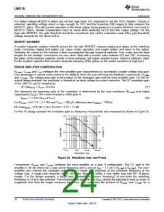
PSW = 0.5 x VIN x IO x (tR + tF) x fSW
where
•
tR and tF are the rise and fall times of the MOSFET
(30)
Switching loss is calculated for the high-side MOSFET only. Switching loss in the low-side MOSFET is negligible
because the body diode of the low-side MOSFET turns on before the MOSFET itself, minimizing the voltage from
drain to source before turn-on. For this example, the maximum drain-to-source voltage applied to either MOSFET
is 60V. VCC provides the drive voltage at the gate of the MOSFETs. The selected MOSFETs must be able to
withstand 60V plus any ringing from drain to source, and be able to handle at least VCC plus ringing from gate to
source. A good choice of MOSFET for the 60V input design example is the Si7850DP. It has an RDS(ON) of 20
mΩ, total gate charge of 14 nC, and rise and fall times of 10 ns and 12 ns respectively. In applications where a
high step-down ratio is maintained for normal operation, efficiency may be optimized by choosing a high-side
MOSFET with lower Qg, and low-side MOSFET with lower RDS(ON)
.
Copyright © 2007–2013, Texas Instruments Incorporated
Submit Documentation Feedback
23
Product Folder Links: LM5116

 TI [ TEXAS INSTRUMENTS ]