LM5116
SNVS499G –FEBRUARY 2007–REVISED MARCH 2013
www.ti.com
For higher voltage MOSFETs which are not true logic level, it is important to use the UVLO feature. Choose a
minimum operating voltage which is high enough for VCC and the bootstrap (HB) supply to fully enhance the
MOSFET gates. This will prevent operation in the linear region during power-on or power-off which can result in
MOSFET failure. Similar consideration must be made when powering VCCX from the output voltage. For the
high-side MOSFET, the gate threshold should be considered and careful evaluation made if the gate threshold
voltage exceeds the HO driver UVLO.
MOSFET SNUBBER
A resistor-capacitor snubber network across the low-side MOSFET reduces ringing and spikes at the switching
node. Excessive ringing and spikes can cause erratic operation and couple spikes and noise to the output.
Selecting the values for the snubber is best accomplished through empirical methods. First, make sure the lead
lengths for the snubber connections are very short. Start with a resistor value between 5Ω and 50Ω. Increasing
the value of the snubber capacitor results in more damping, but higher snubber losses. Select a minimum value
for the snubber capacitor that provides adequate damping of the spikes on the switch waveform at high load.
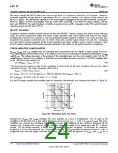
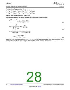
ERROR AMPLIFIER COMPENSATION
RCOMP, CCOMP and CHF configure the error amplifier gain characteristics to accomplish a stable voltage loop gain.
One advantage of current mode control is the ability to close the loop with only two feedback components, RCOMP
and CCOMP. The voltage loop gain is the product of the modulator gain and the error amplifier gain. For the 5V
output design example, the modulator is treated as an ideal voltage-to-current converter. The DC modulator gain
of the LM5116 can be modeled as:
DC Gain(MOD) = RLOAD / (A x RS)
(31)
The dominant low frequency pole of the modulator is determined by the load resistance (RLOAD) and output
capacitance (COUT). The corner frequency of this pole is:
fP(MOD) = 1 / (2π x RLOAD x COUT
)
(32)
For RLOAD = 5V / 7A = 0.714Ω and COUT = 320 µF (effective) then fP(MOD) = 700 Hz
DC Gain(MOD) = 0.714Ω / (10 x 10 mΩ) = 7.14 = 17 dB
For the 5V design example the modulator gain vs. frequency characteristic was measured as shown in Figure 36.
Figure 36. Modulator Gain and Phase
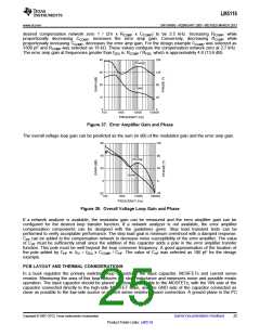
Components RCOMP and CCOMP configure the error amplifier as a type II configuration. The DC gain of the
amplifier is 80 dB which has a pole at low frequency and a zero at fZEA = 1 / (2π x RCOMP x CCOMP). The error
amplifier zero cancels the modulator pole leaving a single pole response at the crossover frequency of the
voltage loop. A single pole response at the crossover frequency yields a very stable loop with 90° of phase
margin. For the design example, a target loop bandwidth (crossover frequency) of one-tenth the switching
frequency or 25 kHz was selected. The compensation network zero (fZEA) should be selected at least an order of
magnitude less than the target crossover frequency. This constrains the product of RCOMP and CCOMP for a
24
Submit Documentation Feedback
Copyright © 2007–2013, Texas Instruments Incorporated
Product Folder Links: LM5116

 TI [ TEXAS INSTRUMENTS ]