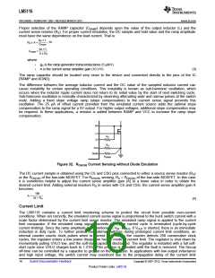
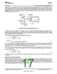
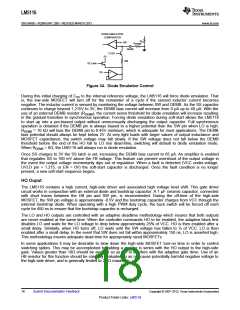
LM5116
SNVS499G –FEBRUARY 2007–REVISED MARCH 2013
www.ti.com
5V
5V
1 -
x
= 6.5mH
L =
60V
0.4 x 7A x 250kHz
(9)
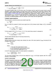
The nearest standard value of 6 µH will be used. The inductor must be rated for the peak current to prevent
saturation. During normal operation, the peak current occurs at maximum load current plus maximum ripple.
During overload conditions with properly scaled component values, the peak current is limited to VCS(TH) / RS
(See CURRENT SENSE RESISTOR). At the maximum input voltage with a shorted output, the valley current
must fall below VCS(TH) / RS before the high-side MOSFET is allowed to turn on. The peak current in steady state
will increase to VIN(MAX) x tON(min) / L above this level. The chosen inductor must be evaluated for this condition,
especially at elevated temperature where the saturation current rating may drop significantly.
CURRENT SENSE RESISTOR
The current limit is set by the current sense resistor value (RS).
VCS(TH)
ILIM
=
RS
(10)
For a 5V output, the maximum current sense signal occurs at the minimum input voltage, so RS is calculated
from:
VCS(TH)
RS
Ç
VOUT
VOUT
x 1 +
IO +
VIN(MIN)
2 x L x fSW
(11)
(12)
For this example VCCX = 0V, so VCS(TH) = 0.11V. The current sense resistor is calculated as:
0.11V
0.011W
Ç
RS Ç
5V
5V
7V
x
1 +
7A +
2 x 6 mH x 250 kHz
The next lowest standard value of 10 mΩ was chosen for RS.
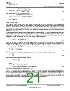
RAMP CAPACITOR
With the inductor and sense resistor value selected, the value of the ramp capacitor (CRAMP) necessary for the
emulation ramp circuit is:
gm x L
CRAMP
,
A x RS
where
•
•
•
L is the value of the output inductor in Henrys
gm is the ramp generator transconductance (5 µA/V)
A is the current sense amplifier gain (10 V/V)
(13)
(14)
For the 5V output design example, the ramp capacitor is calculated as:
5 mA/V x 6 mH
= 300 pF
CRAMP
=
10V/V x 10 mW
The next lowest standard value of 270 pF was selected for CRAMP. A COG type capacitor with 5% or better
tolerance is recommended.
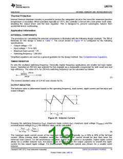
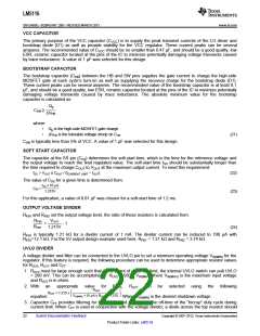
OUTPUT CAPACITORS
The output capacitors smooth the inductor ripple current and provide a source of charge for transient loading
conditions. For this design example, five 100 µF ceramic capacitors where selected. Ceramic capacitors provide
very low equivalent series resistance (ESR), but can exhibit a significant reduction in capacitance with DC bias.
From the manufacturer’s data, the ESR at 250 kHz is 2 mΩ / 5 = 0.4 mΩ, with a 36% reduction in capacitance at
5V. This is verified by measuring the output ripple voltage and frequency response of the circuit. The
fundamental component of the output ripple voltage is calculated as:
20
Submit Documentation Feedback
Copyright © 2007–2013, Texas Instruments Incorporated
Product Folder Links: LM5116

 TI [ TEXAS INSTRUMENTS ]