LM5116
www.ti.com
SNVS499G –FEBRUARY 2007–REVISED MARCH 2013
2
1
ESR2 +
DVOUT = IPP
x
€
8 x fSW x COUT
(15)
With typical values for the 5V design example:
2
1
DVOUT = 3A x 0.4 mW2 +
8 x 250 kHz x 320 mF
DVOUT = 4.8 mV
(16)
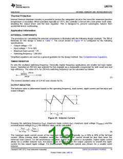
INPUT CAPACITORS
The regulator supply voltage has a large source impedance at the switching frequency. Good quality input
capacitors are necessary to limit the ripple voltage at the VIN pin while supplying most of the switch current
during the on-time. When the buck switch turns on, the current into the switch steps to the valley of the inductor
current waveform, ramps up to the peak value, and then drops to zero at turn-off. The input capacitors should be
selected for RMS current rating and minimum ripple voltage. A good approximation for the required ripple current
rating is IRMS > IOUT / 2.
Quality ceramic capacitors with a low ESR were selected for the input filter. To allow for capacitor tolerances and
voltage rating, four 2.2 µF, 100V ceramic capacitors were used for the typical application circuit. With ceramic
capacitors, the input ripple voltage will be triangular and peak at 50% duty cycle. Taking into account the
capacitance change with DC bias, the input ripple voltage is approximated as:
IOUT
7A
DVIN
=
=
= 1V
4 x 250 kHz x 7 mF
4 x fSW x CIN
(17)
When the converter is connected to an input power source, a resonant circuit is formed by the line impedance
and the input capacitors. If step input voltage transients are expected near the maximum rating of the LM5116, a
careful evaluation of the ringing and possible overshoot at the device VIN pin should be completed. To minimize
overshoot make CIN > 10 x LIN. The characteristic source impedance and resonant frequency are:
LIN
1
fS
=
ZS
=
2p
CIN
LIN x CIN
(18)
(19)
The converter exhibits a negative input impedance which is lowest at the minimum input voltage:
2
VIN
ZIN = -
POUT
The damping factor for the input filter is given by:
ZS
RIN + ESR
ZS
1
2
d =
+
ZIN
where
•
•
RIN is the input wiring resistance
ESR is the series resistance of the input capacitors
(20)
The term ZS / ZIN will always be negative due to ZIN.
When δ = 1, the input filter is critically damped. This may be difficult to achieve with practical component values.
With δ < 0.2, the input filter will exhibit significant ringing. If δ is zero or negative, there is not enough resistance
in the circuit and the input filter will sustain an oscillation. When operating near the minimum input voltage, an
aluminum electrolytic capacitor across CIN may be needed to damp the input for a typical bench test setup. Any
parallel capacitor should be evaluated for its RMS current rating. The current will split between the ceramic and
aluminum capacitors based on the relative impedance at the switching frequency.
Copyright © 2007–2013, Texas Instruments Incorporated
Submit Documentation Feedback
21
Product Folder Links: LM5116

 TI [ TEXAS INSTRUMENTS ]