LM5116
www.ti.com
SNVS499G –FEBRUARY 2007–REVISED MARCH 2013
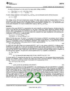
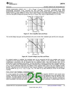
desired compensation network zero 1 / (2π x RCOMP x CCOMP) to be 2.5 kHz. Increasing RCOMP, while
proportionally decreasing CCOMP, increases the error amp gain. Conversely, decreasing RCOMP while
proportionally increasing CCOMP, decreases the error amp gain. For the design example CCOMP was selected as
3300 pF and RCOMP was selected as 18 kΩ. These values configure the compensation network zero at 2.7 kHz.
The error amp gain at frequencies greater than fZEA is: RCOMP / RFB2, which is approximately 4.8 (13.6 dB).
Figure 37. Error Amplifier Gain and Phase
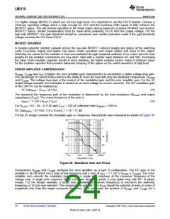
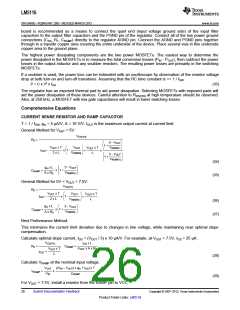
The overall voltage loop gain can be predicted as the sum (in dB) of the modulator gain and the error amp gain.
Figure 38. Overall Voltage Loop Gain and Phase
If a network analyzer is available, the modulator gain can be measured and the error amplifier gain can be
configured for the desired loop transfer function. If a network analyzer is not available, the error amplifier
compensation components can be designed with the guidelines given. Step load transient tests can be
performed to verify acceptable performance. The step load goal is minimum overshoot with a damped response.
CHF can be added to the compensation network to decrease noise susceptibility of the error amplifier. The value
of CHF must be sufficiently small since the addition of this capacitor adds a pole in the error amplifier transfer
function. This pole must be well beyond the loop crossover frequency. A good approximation of the location of
the pole added by CHF is: fP2 = fZEA x CCOMP / CHF. The value of CHF was selected as 100 pF for the design
example.
PCB LAYOUT AND THERMAL CONSIDERATIONS
In a buck regulator the primary switching loop consists of the input capacitor, MOSFETs and current sense
resistor. Minimizing the area of this loop reduces the stray inductance and minimizes noise and possible erratic
operation. The input capacitor should be placed as close as possible to the MOSFETs, with the VIN side of the
capacitor connected directly to the high-side MOSFET drain, and the GND side of the capacitor connected as
close as possible to the low-side source or current sense resistor ground connection. A ground plane in the PC
Copyright © 2007–2013, Texas Instruments Incorporated
Submit Documentation Feedback
25
Product Folder Links: LM5116

 TI [ TEXAS INSTRUMENTS ]