LM5116
www.ti.com
SNVS499G –FEBRUARY 2007–REVISED MARCH 2013
Thermal Protection
Internal thermal shutdown circuitry is provided to protect the integrated circuit in the event the maximum junction
temperature is exceeded. When activated, typically at 170°C, the controller is forced into a low power reset state,
disabling the output driver and the bias regulator. This is designed to prevent catastrophic failures from
accidental device overheating.
Application Information
EXTERNAL COMPONENTS
The procedure for calculating the external components is illustrated with the following design example. The Bill of
Materials for this design is listed in Table 1. The circuit shown in Figure 41 is configured for the following
specifications:
•
•
•
•
Output voltage = 5V
Input voltage = 7V to 60V
Maximum load current = 7A
Switching frequency = 250 kHz
Simplified equations are used as a general guideline for the design method. See Comprehensive Equations.
TIMING RESISTOR
RT sets the oscillator switching frequency. Generally, higher frequency applications are smaller but have higher
losses. Operation at 250 kHz was selected for this example as a reasonable compromise for both small size and
high efficiency. The value of RT for 250 kHz switching frequency can be calculated as follows:
1
- 450 ns
250 kHz
= 12.5 kW
RT =
284 pF
(7)
The nearest standard value of 12.4 kΩ was chosen for RT.
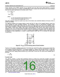
OUTPUT INDUCTOR
The inductor value is determined based on the operating frequency, load current, ripple current and the input and
output voltages.
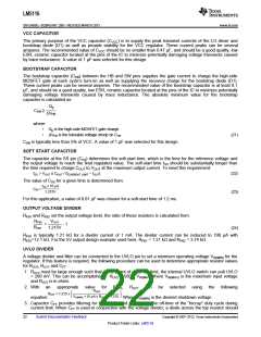
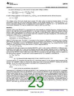
I
I
PP
O
0
1
T =
f
SW
Figure 35. Inductor Current
Knowing the switching frequency (fSW), maximum ripple current (IPP), maximum input voltage (VIN(MAX)) and the
nominal output voltage (VOUT), the inductor value can be calculated:
VOUT
VOUT
VIN(MAX)
1 -
x
L =
IPP x fSW
(8)
The maximum ripple current occurs at the maximum input voltage. Typically, IPP is 20% to 40% of the full load
current. When running diode emulation mode, the maximum ripple current should be less than twice the
minimum load current. For full synchronous operation, higher ripple current is acceptable. Higher ripple current
allows for a smaller inductor size, but places more of a burden on the output capacitor to smooth the ripple
current for low output ripple voltage. For this example, 40% ripple current was chosen for a smaller sized
inductor.
Copyright © 2007–2013, Texas Instruments Incorporated
Submit Documentation Feedback
19
Product Folder Links: LM5116

 TI [ TEXAS INSTRUMENTS ]