LM5116
www.ti.com
SNVS499G –FEBRUARY 2007–REVISED MARCH 2013
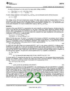
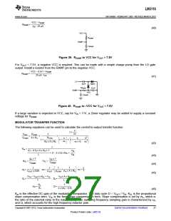
VCC - VRAMP
RRAMP
=
IOS - 25 mA
(40)
VCC
R
RAMP
RAMP
C
RAMP
Figure 39. RRAMP to VCC for VOUT > 7.5V
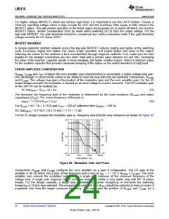
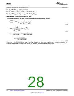
For VOUT < 7.5V, a negative VCC is required. This can be made with a simple charge pump from the LO gate
output. Install a resistor from the RAMP pin to the negative VCC.
VCC œ 0.5V + VRAMP
RRAMP
=
25 mA - IOS
(41)
LO
10 nF
1N914
10 nF
R
RAMP
RAMP
-VCC
RAMP
C
Figure 40. RRAMP to -VCC for VOUT < 7.5V
If a large variation is expected in VCC, say for VIN < 11V, a Zener regulator may be added to supply a constant
voltage for RRAMP
.
MODULATOR TRANSFER FUNCTION
The following equations can be used to calculate the control-to-output transfer function:
s
wZ
1 +
RLOAD
1
VOUT
x
x
=
s
wP
s
s2
A x RS
VCOMP
RLOAD
x
1 +
1 +
+
1 +
2
wn x Q
wn
Km x A x RS
(42)
1
Km
=
(D œ 0.5) x A x RS x T
VSL
+ (1 - 2 x D) x KSL
+
L
VIN
(43)
(44)
gm x T
IOS x T
CRAMP
VSL
=
KSL
=
CRAMP
p
T
1
1
1
1
x
+
wn =
wP =
wZ =
Km x A x RS
COUT x ESR
COUT
RLOAD
(45)
(VIN œ VOUT) x KSL + VSL
VIN x A x RS
L
Se =
Sn =
T
1
Se
mC =
Sn
Q =
p x (mC œ 0.5)
(46)
Km is the effective DC gain of the modulating comparator. The duty cycle D = VOUT / VIN. KSL is the proportional
slope compensation term. VSL is the fixed slope compensation term. Slope compensation is set by mc, which is
the ratio of the external ramp to the natural ramp. The switching frequency sampling gain is characterized by ωn
and Q, which accounts for the high frequency inductor pole.
Copyright © 2007–2013, Texas Instruments Incorporated
Submit Documentation Feedback
27
Product Folder Links: LM5116

 TI [ TEXAS INSTRUMENTS ]