DRV8301-Q1
www.ti.com
SLOS842 –SEPTEMBER 2013
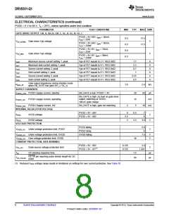
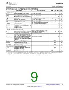
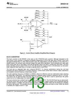
GATE TIMING AND PROTECTION CHARACTERISTICS
PARAMETER
TEST CONDITIONS
MIN TYP
MAX UNIT
TIMING, OUTPUT PINS
tpd,If-O
tpd,Ir-O
Td_min
Tdtp
Positive input falling to GH_x falling
Positive input rising to GL_x falling
Minimum dead time after hand shaking(1)
Dead Time
CL=1nF, 50% to 50%
CL=1nF, 50% to 50%
45
45
ns
ns
50
ns
ns
ns
ns
With RDTC set to different values
CL=1nF, 10% to 90%
50
25
25
500
tGDr
Rise time, gate drive output
Fall time, gate drive output
tGDF
CL=1nF, 90% to 10%
Not including handshake communication.
Hiz to on state, output of gate driver
TON_MIN
Minimum on pulse
50
ns
Propagation delay matching between high
side and low side
Tpd_match
Tdt_match
5
5
ns
ns
Deadtime matching
TIMING, PROTECTION AND CONTROL
PVDD is up before start up, all charge
pump caps and regulator caps as in
recommended condition
Start up time, from EN_GATE active high
to device ready for normal operation
tpd,R_GATE-OP
5
10
10
ms
us
If EN_GATE goes from high to low and
back to high state within quick reset time,
it will only reset all faults and gate driver
without powering down charge pump,
current amp, and related internal voltage
regulators.
tpd,R_GATE-Quick
Maximum low pulse time
tpd,E-L
Delay, error event to all gates low
Delay, error event to FAULT low
200
200
ns
ns
tpd,E-FAULT
Junction temperature for resetting over
temperature warning
OTW_CLR
115
°C
°C
°C
Junction temperature for over
temperature warning and resetting over
temperature shut down
OTW_SET/OTSD
_CLR
130
Junction temperature for over
temperature shut down
OTSD_SET
150
(1) Dead time programming definition: Adjustable delay from GH_x falling edge to GL_X rising edge, and GL_X falling edge to GH_X rising
edge. This is a minimum dead-time insertion. It is not added to the value set by the microcontroller externally.
Copyright © 2013, Texas Instruments Incorporated
Submit Documentation Feedback
9
Product Folder Links: DRV8301-Q1

 TI [ TEXAS INSTRUMENTS ]