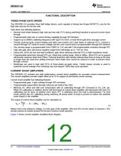
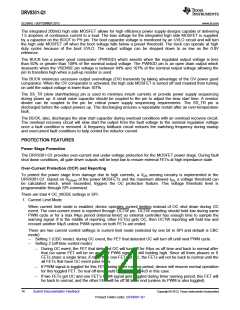
DRV8301-Q1
SLOS842 –SEPTEMBER 2013
www.ti.com
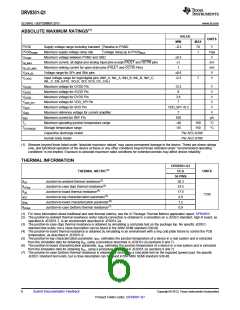
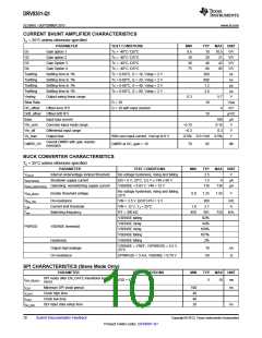
CURRENT SHUNT AMPLIFIER CHARACTERISTICS
TC = 25°C unless otherwise specified
PARAMETER
Gain option 1
TEST CONDITIONS
MIN
9.5
18
TYP
10
MAX UNIT
G1
Tc = -40°C-125°C
10.5
21
V/V
V/V
V/V
V/V
ns
G2
Gain option 2
Tc = -40°C-125°C
20
G3
Gain Option 3
Tc = -40°C-125°C
38
40
42
G4
Gain Option 4
Tc = -40°C-125°C
75
80
85
Tsettling
Tsettling
Tsettling
Tsettling
Vswing
Slew Rate
DC_offset
Drift_offset
Ibias
Settling time to 1%
Settling time to 1%
Settling time to 1%
Settling time to 1%
Output swing linear range
Tc = 0-60°C, G = 10, Vstep = 2 V
Tc = 0-60°C, G = 20, Vstep = 2 V
Tc = 0-60°C, G = 40, Vstep = 2 V
Tc = 0-60°C, G = 80, Vstep = 2 V
300
600
1.2
2.4
ns
µs
µs
0.3
5.7
4
V
G = 10
10
10
V/µs
mV
µV/C
µA
V
Offset error RTI
G = 10 with input shorted
Offset drift RTI
Input bias current
Common input mode range
Differential input range
Output bias
100
0.15
0.3
Vin_com
Vin_dif
Vo_bias
–0.15
–0.3
V
With zero input current, Vref up to 6 V
CMRR at DC, gain = 10
–0.5% 0.5×Vref
0.5%
V
Overall CMRR with gain resistor
mismatch
CMRR_OV
70
85
dB
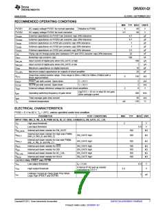
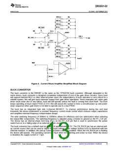
BUCK CONVERTER CHARACTERISTICS
TC = 25°C unless otherwise specified
PARAMETER
TEST CONDITIONS
MIN
TYP
2.5
MAX UNIT
VUVLO
Internal undervoltage lockout threshold
Shutdown supply current
No voltage hysteresis, rising and falling
EN = 0 V, 25°C, 3.5 V ≤ VIN ≤ 60 V
VSENSE = 0.83 V, VIN = 12 V
V
ISD(PVDD2)
1.3
4
µA
µA
INON_SW(PVDD2) Operating: nonswitching supply current
116
136
No voltage hysteresis, rising and falling,
25°C
VEN_BUCK
Enable threshold voltage
0.9
1.25
1.55
V
RDS_ON
ILIM
On-resistance
VIN = 3.5 V, BOOT-PH = 3 V
VIN = 12 V, TJ = 25°C
RT = 200 kΩ
300
2.7
mΩ
A
Current limit threshold
Switching frequency
1.8
Fsw
450
581
720
kHz
VSENSE falling
92%
94%
109%
107%
2%
VSENSE rising
PWRGD
VSENSE threshold
VSENSE rising
VSENSE falling
Hysteresis
VSENSE falling
VSENSE = VREF, V(PWRGD) = 5.5 V,
25°C
Output high leakage
On resistance
10
50
nA
I(PWRGD) = 3 mA, VSENSE < 0.79 V
Ω
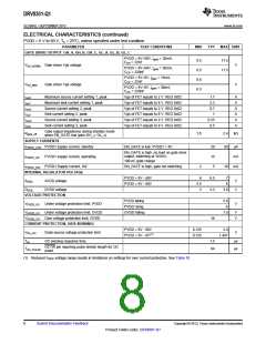
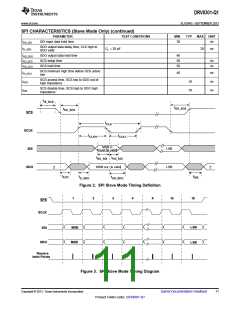
SPI CHARACTERISTICS (Slave Mode Only)
PARAMETER
TEST CONDITIONS
MIN
TYP
MAX UNIT
SPI ready after EN_GATE transitions to
HIGH
tSPI_READY
PVDD > 6 V
5
10
ms
ns
tCLK
Minimum SPI clock period
Clock high time
100
40
tCLKH
tCLKL
tSU_SDI
Clock low time
40
SDI input data setup time
20
ns
10
Submit Documentation Feedback
Copyright © 2013, Texas Instruments Incorporated
Product Folder Links: DRV8301-Q1

 TI [ TEXAS INSTRUMENTS ]