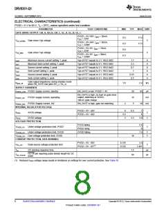
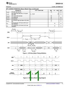
DRV8301-Q1
SLOS842 –SEPTEMBER 2013
www.ti.com
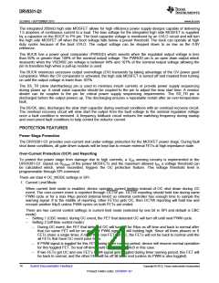
FUNCTIONAL DESCRIPTION
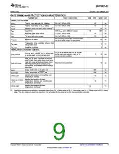
THREE-PHASE GATE DRIVER
The DRV8301-Q1 provides three half bridge drivers, each capable of driving two N-type MOSFETs, one for the
high-side and one for the low side.
Gate driver has following features:
•
Internal hand shake between high side and low side FETs during switching transition to prevent current shoot
through.
•
•
•
Programmable slew rate or current driving capability through SPI interface.
Support up to 200kHz switching frequency with Qg(TOT)=25nC or total 30mA gate drive average current
Provide cycle-by-cycle current limiting and latch over-current (OC) shut down of external FETs. Current is
sensed through FET drain-to-source voltage and the over-current level is programmable through SPI interface
•
•
•
•
Vds sensing range is programmable from 0.060V to 2.4V and with 5 bit programmable resolution through SPI.
High side gate drive will survive negative output from half bridge up to –10V for 10ns
During EN_GATE pin low and fault conditions, gate driver will keep external FETs in high impedance mode.
Programmable dead time through DTC pin. Dead time control range: 50ns to 500ns. Short DTC pin to ground
will provide minimum dead time (50ns). External dead time will override internal dead time as long as the time
is longer than the dead time setting (minimum hand shake time cannot be reduced in order to prevent shoot
through current).
•
Bootstraps are used in high side FETs of three-phase pre-gate driver. Trickle charge circuitry is used to
replenish current leakage from bootstrap cap and support 100% duty cycle operation.
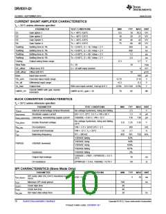
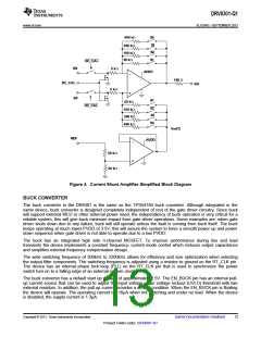
CURRENT SHUNT AMPLIFIERS
The DRV8301-Q1 includes two high performance current shunt amplifiers for accurate current measurement.
The current amplifiers provide output offset up to 3V to support bi-directional current sensing.
Current shunt amplifier has following features:
•
•
•
Programmable gain: 4 gain settings through SPI command
Programmable output offset through reference pin (half of the Vref)
Minimize DC offset and drift over temperature with dc calibrating through SPI command or DC_CAL pin.
When DC calibration is enabled, device will short input of current shunt amplifier and disconnect the load. DC
calibrating can be done at anytime even when FET is switching since the load is disconnected. For best
result, perform the DC calibrating during switching off period when no load is present to reduce the potential
noise impact to the amplifier.
The output of current shunt amplifier can be calculated as:
VREF
VO
=
- G ´ SN - SPX
X
(
)
2
(1)
Where Vref is the reference voltage, G is the gain of the amplifier; SNx and SPx are the inputs of channel x. SPx
should connect to resistor ground for the best common mode rejection.
Figure 4 shows current amplifier simplified block diagram.
12
Submit Documentation Feedback
Copyright © 2013, Texas Instruments Incorporated
Product Folder Links: DRV8301-Q1

 TI [ TEXAS INSTRUMENTS ]