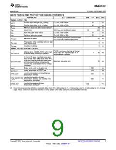
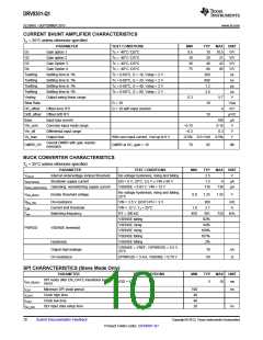
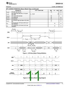
DRV8301-Q1
www.ti.com
SLOS842 –SEPTEMBER 2013
400 kW
S4
S3
S2
200 kW
100 kW
50 kW
S1
DC_CAL
SN
5 kW
5 kW
AVDD
_
100 W
DC_CAL
SO
+
SP
S1
50 kW
100 kW
200 kW
400 kW
DC CAL
_
S2
S3
S4
Vref/2
REF
AVDD
_
+
50 kW
50 kW
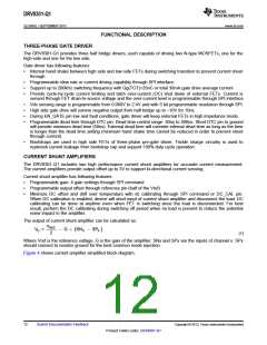
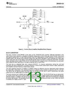
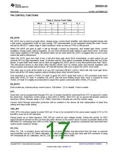
Figure 4. Current Shunt Amplifier Simplified Block Diagram
BUCK CONVERTER
The buck converter in the DR8301 is the same as the TPS54160 buck converter. Although integrated in the
same device, buck converter is designed completely independent of rest of the gate driver circuitry. Since buck
will support external MCU or other external power need, the independency of buck operation is very critical for a
reliable system; this will give buck minimum impact from gate driver operations. Some examples are: when gate
driver shuts down due to any failure, buck will still operate unless the fault is coming from buck itself. The buck
keeps operating at much lower PVDD of 3.5V, this will assure the system to have a smooth power up and power
down sequence when gate driver is not able to operate due to a low PVDD.
The buck has an integrated high side n-channel MOSFET. To improve performance during line and load
transients the device implements a constant frequency, current mode control which reduces output capacitance
and simplifies external frequency compensation design.
The wide switching frequency of 300kHz to 2200kHz allows for efficiency and size optimization when selecting
the output filter components. The switching frequency is adjusted using a resistor to ground on the RT_CLK pin.
The device has an internal phase lock loop (PLL) on the RT_CLK pin that is used to synchronize the power
switch turn on to a falling edge of an external system clock.
The buck converter has a default start up voltage of approximately 2.5V. The EN_BUCK pin has an internal pull-
up current source that can be used to adjust the input voltage under voltage lockout (UVLO) threshold with two
external resistors. In addition, the pull up current provides a default condition. When the EN_BUCK pin is floating
the device will operate. The operating current is 116µA when not switching and under no load. When the device
is disabled, the supply current is 1.3µA.
Copyright © 2013, Texas Instruments Incorporated
Submit Documentation Feedback
13
Product Folder Links: DRV8301-Q1

 TI [ TEXAS INSTRUMENTS ]