DRV8301-Q1
SLOS842 –SEPTEMBER 2013
www.ti.com
UNITS
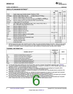
ABSOLUTE MAXIMUM RATINGS(1)
VALUE
MIN
MAX
70
PVDD
Supply voltage range including transient Relative to PGND
Maximum supply voltage ramp rate Voltage rising up to PVDDMAX
–0.3
V
V/µs
V
PVDDRAMP
VPGND
1
Maximum voltage between PGND and GND
±0.3
±1
IIN_MAX
Maximum current, all digital and analog input pins except FAULT and OCTW pins
Maximum sinking current for open drain pins (FAULT and OCTW Pins)
Voltage range for SPx and SNx pins
mA
mA
V
IIN_OD_MAX
VOPA_IN
VLOGIC
7
±0.6
-0.3
Input voltage range for logic/digital pins (INH_A, INL_A, INH_B, INL_B, INH_C,
INL_C, EN_GATE, SCLK, SDI, SCS, DC_CAL)
7
V
VGVDD
VAVDD
VDVDD
VVDD_SPI
VSDO
Maximum voltage for GVDD Pin
Maximum voltage for AVDD Pin
Maximum voltage for DVDD Pin
Maximum voltage for VDD_SPI Pin
Maximum voltage for SDO Pin
Maximum reference voltage for current amplifier
Maximum current for REF Pin
13.2
V
V
8
3.6
V
7
V
VDD_SPI +0.3
V
VREF
7
V
IREF
100
–40
–55
µA
°C
°C
TJ
Maximum operating junction temperature range
Storage temperature range
150
150
TSTORAGE
Capacitive discharge model
Per AEC-Q100
Per AEC-Q100
Human body model
(1) Stresses beyond those listed under “absolute maximum ratings” may cause permanent damage to the device. These are stress ratings
only, and functional operation of the device at these or any other conditions beyond those indicated under “recommended operating
conditions” is not implied. Exposure to absolute-maximum-rated conditions for extended periods may affect device reliability.
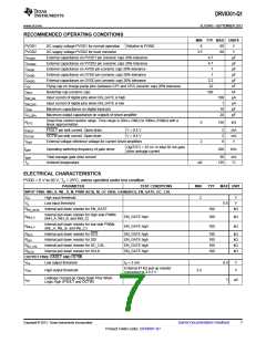
THERMAL INFORMATION
DRV8301-Q1
THERMAL METRIC(1)
DCA
56 PINS
30.3
33.5
17.5
0.9
UNITS
θJA
Junction-to-ambient thermal resistance(2)
Junction-to-case (top) thermal resistance(3)
Junction-to-board thermal resistance(4)
Junction-to-top characterization parameter(5)
Junction-to-board characterization parameter(6)
Junction-to-case (bottom) thermal resistance(7)
θJCtop
θJB
°C/W
ψJT
ψJB
7.2
θJCbot
0.9
(1) For more information about traditional and new thermal metrics, see the IC Package Thermal Metrics application report, SPRA953.
(2) The junction-to-ambient thermal resistance under natural convection is obtained in a simulation on a JEDEC-standard, high-K board, as
specified in JESD51-7, in an environment described in JESD51-2a.
(3) The junction-to-case (top) thermal resistance is obtained by simulating a cold plate test on the package top. No specific JEDEC-
standard test exists, but a close description can be found in the ANSI SEMI standard G30-88.
(4) The junction-to-board thermal resistance is obtained by simulating in an environment with a ring cold plate fixture to control the PCB
temperature, as described in JESD51-8.
(5) The junction-to-top characterization parameter, ψJT, estimates the junction temperature of a device in a real system and is extracted
from the simulation data for obtaining θJA, using a procedure described in JESD51-2a (sections 6 and 7).
(6) The junction-to-board characterization parameter, ψJB, estimates the junction temperature of a device in a real system and is extracted
from the simulation data for obtaining θJA , using a procedure described in JESD51-2a (sections 6 and 7).
(7) The junction-to-case (bottom) thermal resistance is obtained by simulating a cold plate test on the exposed (power) pad. No specific
JEDEC standard test exists, but a close description can be found in the ANSI SEMI standard G30-88.
Spacer
6
Submit Documentation Feedback
Copyright © 2013, Texas Instruments Incorporated
Product Folder Links: DRV8301-Q1

 TI [ TEXAS INSTRUMENTS ]