DRV8301-Q1
www.ti.com
SLOS842 –SEPTEMBER 2013
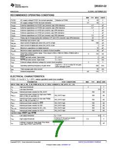
RECOMMENDED OPERATING CONDITIONS
MIN TYP MAX UNITS
PVDD1
PVDD2
CPVDD1
CPVDD2
CAVDD
CDVDD
CGVDD
CCP
DC supply voltage PVDD1 for normal operation
DC supply voltage PVDD2 for buck converter
Relative to PGND
6
60
60
V
3.5
V
External capacitance on PVDD1 pin (ceramic cap) 20% tolerance
External capacitance on PVDD2 pin (ceramic cap) 20% tolerance
External capacitance on AVDD pin (ceramic cap) 20% tolerance
External capacitance on DVDD pin (ceramic cap) 20% tolerance
External capacitance on GVDD pin (ceramic cap) 20% tolerance
Flying cap on charge pump pins (between CP1 and CP2) (ceramic cap) 20% tolerance
Bootstrap cap (ceramic cap)
4.7
4.7
1
µF
µF
µF
µF
µF
nF
nF
µA
µA
pF
pF
1
2.2
22
100
CBST
IDIN_EN
IDIN_DIS
CDIN
Input current of digital pins when EN_GATE is high
100
1
Input current of digital pins when EN_GATE is low
Maximum capacitance on digital input pin
10
20
CO_OPA
Maximum output capacitance on outputs of shunt amplifier
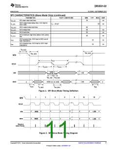
Dead time control resistor range. Time range is 50ns (-GND) to 500ns (150kΩ) with a
linear approximation.
RDTC
0
2
150
kΩ
IFAULT
IOCTW
VREF
FAULT pin sink current. Open-drain
OCTW pin sink current. Open-drain
V = 0.4 V
V = 0.4 V
2
2
6
mA
mA
V
External voltage reference voltage for current shunt amplifiers
Qg(TOT) = 25 nC or total 30 mA gate
drive average current
fgate
Operating switching frequency of gate driver
200
kHz
Igate
TA
Total average gate drive current
Ambient temperature
30
mA
°C
–40
125
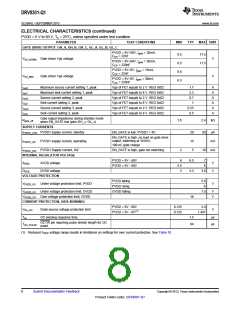
ELECTRICAL CHARACTERISTICS
PVDD = 6 V to 60 V, TC = 25°C, unless specified under test condition
PARAMETER
TEST CONDITIONS
MIN
TYP
MAX UNIT
INPUT PINS: INH_X, INL_X, M_PWM (SCS), M_OC (SDI), GAIN(SDO), EN_GATE, DC_CAL
VIH
High input threshold
2
V
VIL
Low input threshold
0.8
V
REN_GATE
Internal pull down resistor for EN_GATE
100
100
kΩ
Internal pull down resistor for high side PWMs
(INH_A, INH_B, and INH_C)
RINH_X
RINH_X
EN_GATE high
EN_GATE high
kΩ
kΩ
Internal pull down resistor for low side PWMs
(INL_A, INL_B, and INL_C)
100
RSCS
Internal pull down resistor for SCS
Internal pull down resistor for SDI
Internal pull down resistor for DC_CAL
Internal pull down resistor for SCLK
EN_GATE high
EN_GATE high
EN_GATE high
EN_GATE high
100
100
100
100
kΩ
kΩ
kΩ
kΩ
RSDI
RDC_CAL
RSCLK
OUTPUT PINS: FAULT AND OCTW
VOL
Low output threshold
IO = 2 mA
0.4
1
V
V
External 47 kΩ pull up resistor
connected to 3-5.5 V
VOH
High output threshold
2.4
Leakage Current on Open Drain Pins When
Logic High (FAULT and OCTW)
IOH
µA
Copyright © 2013, Texas Instruments Incorporated
Submit Documentation Feedback
7
Product Folder Links: DRV8301-Q1

 TI [ TEXAS INSTRUMENTS ]