DRV8301-Q1
www.ti.com
SLOS842 –SEPTEMBER 2013
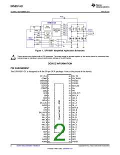
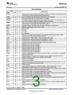
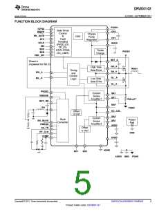
PIN FUNCTIONS
PIN
I/O(1)
DESCRIPTION
NAME
NO.
RT_CLK
1
I
Resistor timing and external clock for buck regulator. Resistor should connect to GND (power pad) with
very short trace to reduce the potential clock jitter due to noise.
COMP
2
3
4
O
I
Buck error amplifier output and input to the output switch current comparator.
Buck output voltage sense pin. Inverting node of error amplifier.
VSENSE
PWRGD
I
An open drain output with external pull-up resistor required. Asserts low if buck output voltage is low
due to thermal shutdown, dropout, over-voltage, or EN_BUCK shut down
OCTW
5
O
Over current or/and over temperature warning indicator. This output is open drain with external pull-up
resistor required. Programmable output mode via SPI registers.
FAULT
DTC
6
7
O
I
Fault report indicator. This output is open drain with external pull-up resistor required.
Dead-time adjustment with external resistor to GND
SCS
8
I
SPI chip select
SPI input
SDI
9
I
SDO
10
11
12
O
I
SPI output
SCLK
DC_CAL
SPI clock signal
I
When DC_CAL is high, device shorts inputs of shunt amplifiers and disconnects loads. DC offset
calibration can be done through external microcontroller.
GVDD
CP1
13
14
15
16
17
18
19
20
21
22
23
P
P
P
I
Internal gate driver voltage regulator. GVDD cap should connect to GND
Charge pump pin 1, ceramic cap should be used between CP1 and CP2
Charge pump pin 2, ceramic cap should be used between CP1 and CP2
Enable gate driver and current shunt amplifiers. Control buck via EN_BUCK pin.
PWM Input signal (high side), half-bridge A
CP2
EN_GATE
INH_A
INL_A
INH_B
INL_B
INH_C
INL_C
DVDD
I
I
PWM Input signal (low side), half-bridge A
I
PWM Input signal (high side), half-bridge B
I
PWM Input signal (low side), half-bridge B
I
PWM Input signal (high side), half-bridge C
I
PWM Input signal (low side), half-bridge C
P
Internal 3.3V supply voltage. DVDD cap should connect to AGND. This is an output, but not specified
to drive external circuitry.
REF
24
I
Reference voltage to set output of shunt amplfiiers with a bias voltage which equals to half of the
voltage set on this pin. Connect to ADC reference in microcontroller.
SO1
25
26
27
O
O
P
Output of current amplifier 1
Output of current amplifier 2
SO2
AVDD
Internal 6V supply voltage, AVDD cap should always be installed and connected to AGND. This is an
output, but not specified to drive external circuitry.
AGND
28
29
P
P
Analog ground pin
PVDD1
Power supply pin for gate driver, current shunt amplifier, and SPI communication. PVDD1 is
independent of buck power supply, PVDD2. PVDD1 cap should connect to GND
SP2
30
I
Input of current amplifier 2 (connecting to positive input of amplifier). Recommend to connect to ground
side of the sense resistor for the best commom mode rejection.
SN2
SP1
31
32
I
I
Input of current amplifier 2 (connecting to negative input of amplifier).
Input of current amplifier 1 (connecting to positive input of amplifier). Recommend to connect to ground
side of the sense resistor for the best commom mode rejection.
SN1
33
34
I
I
Input of current amplifier 1 (connecting to negative input of amplifier).
SL_C
Low-Side MOSFET source connection, half-bridge C. Low-side VDS measured between this pin and
SH_C.
GL_C
SH_C
35
36
O
I
Gate drive output for Low-Side MOSFET, half-bridge C
High-Side MOSFET source connection, half-bridge C. High-side VDS measured between this pin and
PVDD1.
GH_C
37
O
Gate drive output for High-Side MOSFET, half-bridge C
(1) KEY: I =Input, O = Output, P = Power
Copyright © 2013, Texas Instruments Incorporated
Submit Documentation Feedback
3
Product Folder Links: DRV8301-Q1

 TI [ TEXAS INSTRUMENTS ]