DRV8301-Q1
SLOS842 –SEPTEMBER 2013
www.ti.com
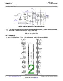
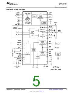
PVDD
DRV8301-Q1
GH_A
GL_A
GH_B
GL_B
GH_C
GL_C
Buck
Converter
Three-Phase
NMOS Gate
Driver
MOTOR
PWM
Vs
3 or 6
Control
and
SPI
Error
Reporting
Protection
Logic
Motor
Controller
_
ADC1
Vref
offset
+
_
ADC2
offset
+
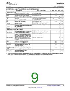
Figure 1. DRV8301 Simplified Application Schematic
These devices have limited built-in ESD protection. The leads should be shorted together or the device placed in conductive foam
during storage or handling to prevent electrostatic damage to the MOS gates.
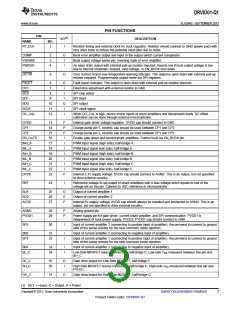
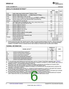
DEVICE INFORMATION
PIN ASSIGNMENT
The DRV8301-Q1 is designed to fit the 56-pin DCA package. Here is the pinout of the device.
RT_CLK 1
COMP 2
56 SS_TR
55 EN_BUCK
54 PVDD2
53 PVDD2
VSENSE 3
PWRGD 4
OCTW 5
FAULT 6
DTC 7
52 BST_BK
51 PH
50 PH
SCS 8
49 VDD_SPI
4 8 BST_A
47 GH_A
46 SH_A
45 GL_A
44 SL_A
43 BST_B
42 GH_B
41 SH_B
40 GL_B
39 SL_B
38 BST_C
37 GH_C
36 SH_C
35 GL_C
34 SL_C
33 SN1
SDI 9
SDO 10
SCLK 11
DC_CAL 12
GVDD 13
CP1 14
CP2 15
EN_GATE 16
INH_A 17
INL_A 18
INH_B 19
INL_B 20
INH_C 21
INL_C 22
DVDD 23
REF 24
SO1 25
32 SP1
SO2 26
31 SN2
AVDD 27
AGND 28
30 SP2
29 PVDD1
2
Submit Documentation Feedback
Copyright © 2013, Texas Instruments Incorporated
Product Folder Links: DRV8301-Q1

 TI [ TEXAS INSTRUMENTS ]