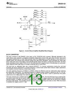
DRV8301-Q1
www.ti.com
SLOS842 –SEPTEMBER 2013
PIN CONTROL FUNCTIONS
Table 2. Device Truth Table
INH_X
INL_X
GH_X
GL_X
1
1
0
0
1
0
1
0
L
H
L
L
L
H
L
L
EN_GATE
EN_GATE low is used to put gate driver, charge pump, current shunt amplifier, and internal regulator blocks into
a low power consumption mode to save energy. SPI communication is not supported during this state. Device
will put the MOSFET output stage to high impedance mode as long as PVDD is still present.
When EN_GATE pin goes to high, it will go through a power up sequence, and enable gate driver, current
amplifiers, charge pump, internal regulator, etc and reset all latched faults related to gate driver block. It will also
reset status registers in SPI table. All latched faults can be reset when EN_GATE is toggled after an error event
unless the fault is still present.
When EN_GATE goes from high to low, it will shut down gate driver block immediately, so gate output can put
external FETs in high impedance mode. It will then wait for 10us before completely shutting down the rest of the
blocks. A quick fault reset mode can be done by toggling EN_GATE pin for a very short period (less than 10µS).
This will prevent device to shut down other function blocks such as charge pump and internal regulators and
bring a quicker and simple fault recovery. SPI will still function with such a quick EN_GATE reset mode.
The other way to reset all the faults is to use SPI command (RESET_GATE), which will only reset gate driver
block and all the SPI status registers without shutting down other function blocks.
One exception is to reset a GVDD_OV fault. A quick EN_GATE quick fault reset or SPI command reset won’t
work with GVDD_OV fault. A complete EN_GATE with low level holding longer than 10µS is required to reset
GVDD_OV fault. It is highly recommended to inspect the system and board when GVDD_OV occurs.
EN_BUCK
Buck enable pin, internal pull-up current source. Pull below 1.2V to disable. Float to enable.
DTC
Dead time can be programmed through DTC pin. A resistor should be connected from DTC to ground to control
the dead time. Dead time control range is from 50ns to 500ns. Short DTC pin to ground will provide minimum
dead time (50ns). Resistor range is 0 to 150kΩ. Dead time is linearly set over this resistor range.
Current shoot through prevention protection will be enabled in the device all time independent of dead time
setting and input mode setting.
VDD_SPI
VDD_SPI is the power supply to power SDO pin. It has to be connected to the same power supply (3.3V or 5V)
that MCU uses for its SPI operation.
During power up or down transient, VDD_SPI pin could be zero voltage shortly. During this period, no SDO
signal should be present at SDO pin from any other devices in the system since it causes a parasitic diode in the
DRV8301-Q1 conducting from SDO to VDD_SPI pin as a short. This should be considered and prevented from
system power sequence design.
DC_CAL
When DC_CAL is enabled, device will short inputs of shunt amplifier and disconnect from the load, so external
microcontroller can do a DC offset calibration. DC offset calibration can be also done with SPI command. If using
SPI exclusively for DC calibration, the DC_CAL pin can connected to GND.
Copyright © 2013, Texas Instruments Incorporated
Submit Documentation Feedback
17
Product Folder Links: DRV8301-Q1

 TI [ TEXAS INSTRUMENTS ]