DRV8301-Q1
www.ti.com
SLOS842 –SEPTEMBER 2013
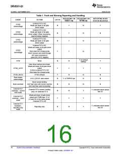
2. OC latch shut down mode
When OC occurs, device will turn off both high side and low side FETs in the same phase if any of the FETs
in that phase has OC.
3. Report only mode
No protection action will be performance in this mode. OC detection will be reported through OCTW pin and
SPI status register. External MCU should take actions based on its own control algorithm. A pulse stretching
of 64µS will be implemented on OCTW pin so controller can have enough time to sense the OC signal.
4. OC disable mode
Device will ignore all the OC detections and will not report them either.
Under-Voltage Protection (UVP)
To protect the power output stage during startup, shutdown and other possible under-voltage conditions, the
DRV8301-Q1 provides power stage under-voltage protection by driving its outputs low whenever PVDD is below
6V (PVDD_UV) or GVDD is below 7.5V (GVDD_UV). When UVP is triggered, the DRV8301-Q1 outputs are
driven low and the external MOSFETs will go to a high impedance state.
Over-Voltage Protection (GVDD_OV)
Device will shut down both gate driver and charge pump if GVDD voltage exceeds 16V to prevent potential issue
related to GVDD or charge pump (e.g. short of external GVDD cap or charge pump). The fault is a latched fault
and can only be reset through a transition on EN_GATE pin.
Over-Temperature Protection
A two-level over-temperature detection circuit is implemented:
•
Level 1: over temperature warning (OTW)
OTW is reported through OCTW pin (over-current-temperature warning) for default setting. OCTW pin can be
set to report OTW or OCW only through SPI command. See SPI Register section.
•
Level 2: over temperature (OT) latched shut down of gate driver and charge pump (OTSD_GATE)
Fault will be reported to FAULT pin. This is a latched shut down, so gate driver will not be recovered
automatically even OT condition is not present anymore. An EN_GATE reset through pin or SPI
(RESET_GATE) is required to recover gate driver to normal operation after temperature goes below a preset
value, tOTSD_CLR
.
SPI operation is still available and register settings will be remaining in the device during OTSD operation as long
as PVDD is still within defined operation range.
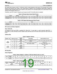
Fault and Protection Handling
The FAULT pin indicates an error event with shut down has occurred such as over-current, over-temperature,
over-voltage, or under-voltage. Note that FAULT is an open-drain signal. FAULT will go high when gate driver is
ready for PWM signal (internal EN_GATE goes high) during start up.
The OCTW pin indicates over current event and over temperature event that not necessary related to shut down.
Following is the summary of all protection features and their reporting structure:
Copyright © 2013, Texas Instruments Incorporated
Submit Documentation Feedback
15
Product Folder Links: DRV8301-Q1

 TI [ TEXAS INSTRUMENTS ]