DRV8301-Q1
www.ti.com
SLOS842 –SEPTEMBER 2013
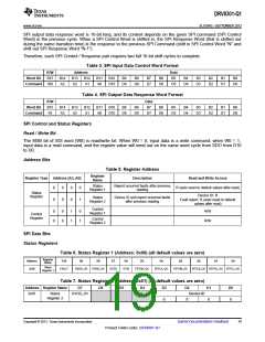
SPI output data response word is 16-bit long, and its content depends on the given SPI command (SPI Control
Word) in the previous cycle. When a SPI Control Word is shifted in, the SPI Response Word (that is shifted out
during the same transition time) is the response to the previous SPI Command (shift in SPI Control Word "N" and
shift out SPI Response Word "N-1").
Therefore, each SPI Control / Response pair requires two full 16-bit shift cycles to complete.
Table 3. SPI Input Data Control Word Format
R/W
B15
W0
Address
Data
B5
Word Bit
B14
A3
B13
B12
A1
B11
A0
B10
D10
B9
D9
B8
D8
B7
D7
B6
D6
B4
D4
B3
D3
B2
D2
B1
D1
B0
D0
Command
A2
D5
Table 4. SPI Output Data Response Word Format
R/W
B15
F0
Data
Word Bit
B14
A3
B13
A2
B12
A1
B11
A0
B10
D10
B9
D9
B8
D8
B7
D7
B6
D6
B5
D5
B4
D4
B3
D3
B2
D2
B1
D1
B0
D0
Command
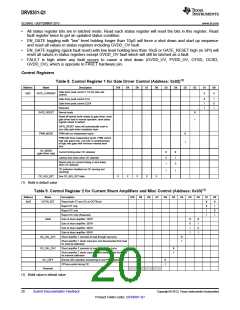
SPI Control and Status Registers
Read / Write Bit
The MSB bit of SDI word (W0) is read/write bit. When W0 = 0, input data is a write command; when W0 = 1,
input data is a read command, and the register value will send out on the same word cycle from SDO from D10
to D0.
Address Bits
Table 5. Register Address
Register
Name
Register Type Address [A3..A0]
Description
Read and Write Access
Status
Register 1
Report occurred faults after previous
reading
0
0
0
0
0
0
0
1
R (auto reset to default values after read)
Status
Register
Device ID: R
Fault report: R (auto reset to default
values after read)
Status
Register 2
Device ID and report occurred faults
after previous reading
Control
Register 1
0
0
0
0
1
1
0
1
R/W
R/W
Control
Register
Control
Register 2
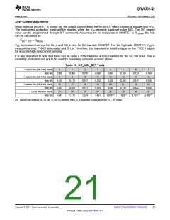
SPI Data Bits
Status Registers
Table 6. Status Register 1 (Address: 0x00) (all default values are zero)
Register
Address
D10
D9
D8
D7
D6
D5
D4
D3
D2
D1
D0
Name
Status
0x00
FAULT
GVDD_UV
PVDD_UV
OTSD
OTW
FETHA_OC
FETLA_OC
FETHB_OC
FETLB_OC FETHC_OC FETLC_OC
Register 1
Table 7. Status Register 2 (Address: 0x01) (all default values are zero)
Address Register Name
D7
D6
D5
D4
D3
D2
Device ID
D1
D0
0x01
Status
GVDD_OV
Register 2
0
0
0
0
Copyright © 2013, Texas Instruments Incorporated
Submit Documentation Feedback
19
Product Folder Links: DRV8301-Q1

 TI [ TEXAS INSTRUMENTS ]