DRV8301-Q1
SLOS842 –SEPTEMBER 2013
www.ti.com
•
•
•
•
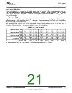
All status register bits are in latched mode. Read each status register will reset the bits in this register. Read
fault register twice to get an updated status condition.
EN_GATE toggling with “low” level holding longer than 10µS will force a shut down and start up sequence
and reset all values in status registers including GVDD_OV fault.
EN_GATE toggling (quick fault reset) with low level holding less than 10uS or GATE_RESET high (in SPI) will
reset all values in status registers except GVDD_OV fault which will still be latched as a fault.
FAULT is high when any fault occurs to cause a shut down (GVDD_UV, PVDD_UV, OTSD, OCSD,
GVDD_OV), which is opposite to FAULT hardware pin.
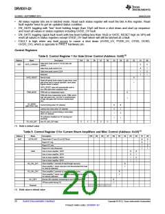
Control Registers
Table 8. Control Register 1 for Gate Driver Control (Address: 0x02)(1)
Address
Name
Description
D10
D9
D8
D7
D6
D5
D4
D3
D2
D1
D0
Gate driver peak current 1.7A (for slew rate
control)
0x02
GATE_CURRENT
0
0
Gate driver peak current 0.7A
Gate driver peak current 0.25A
Reserved
0
1
1
1
0
1
GATE_RESET
PWM_MODE
Normal mode
0
Reset all latched faults related to gate driver, reset
gate driver back to normal operation, reset status
register values to default
1
GATE_RESET value will automatically reset to
zero after gate driver completes reset
PWM with six independent inputs
0
PWM with three independent inputs. PWM control
high side gates only. Low side is complementary
to high side gates with minimum internal dead
time.
1
OC_MODE
(gate driver only)
Current limiting when OC detected
0
0
1
0
1
0
Latched shut down when OC detected
Report only (no current limiting or shut down)
when OC detected
OC protection disabled (no OC sensing and
reporting)
1
1
OC_ADJ_SET
See OC_ADJ_SET table
X
X
X
X
X
(1) Bold is default value
Table 9. Control Register 2 for Current Shunt Amplifiers and Misc Control (Address: 0x03)(1)
Address
Name
Description
D10
D9
D8
D7
D6
D5
D4
D3
D2
D1
0
D0
0
0x03
OCTW_SET
Report both OT and OC at /OCTW pin
Report OT only
0
1
Report OC only
1
0
Report OC Only (Reserved)
Gain of shunt amplifier: 10V/V
Gain of shunt amplifier: 20V/V
Gain of shunt amplifier: 40V/V
Gain of shunt amplifier: 80V/V
Shunt amplifier 1 connects to load through input pins
1
1
GAIN
0
0
1
1
0
1
0
1
DC_CAL_CH1
DC_CAL_CH2
0
Shunt amplifier 1 shorts input pins and disconnected from load
for external calibration
1
Shunt amplifier 2 connects to load through input pins
0
Shunt amplifier 2 shorts input pins and disconnected from load
for external calibration
1
OC_TOFF
Reserved
Normal CBC operation (recovering at next PWM cycle)
Off time control during OC
0
1
(1) Bold value is default value
20
Submit Documentation Feedback
Copyright © 2013, Texas Instruments Incorporated
Product Folder Links: DRV8301-Q1

 TI [ TEXAS INSTRUMENTS ]