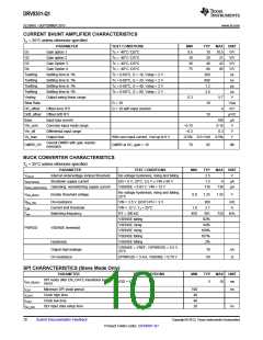
DRV8301-Q1
SLOS842 –SEPTEMBER 2013
www.ti.com
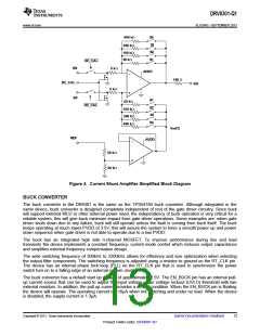
The integrated 200mΩ high side MOSFET allows for high efficiency power supply designs capable of delivering
1.5 amperes of continuous current to a load. The bias voltage for the integrated high side MOSFET is supplied
by a capacitor on the BOOT to PH pin. The boot capacitor voltage is monitored by an UVLO circuit and will turn
the high side MOSFET off when the boot voltage falls below a preset threshold. The buck can operate at high
duty cycles because of the boot UVLO. The output voltage can be stepped down to as low as the 0.8V
reference.
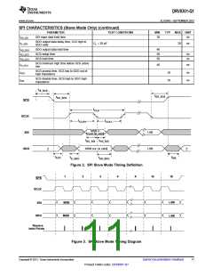
The BUCK has a power good comparator (PWRGD) which asserts when the regulated output voltage is less
than 92% or greater than 109% of the nominal output voltage. The PWRGD pin is an open drain output which
deasserts when the VSENSE pin voltage is between 94% and 107% of the nominal output voltage allowing the
pin to transition high when a pull-up resistor is used.
The BUCK minimizes excessive output overvoltage (OV) transients by taking advantage of the OV power good
comparator. When the OV comparator is activated, the high side MOSFET is turned off and masked from turning
on until the output voltage is lower than 107%.
The SS_TR (slow start/tracking) pin is used to minimize inrush currents or provide power supply sequencing
during power up. A small value capacitor should be coupled to the pin to adjust the slow start time. A resistor
divider can be coupled to the pin for critical power supply sequencing requirements. The SS_TR pin is
discharged before the output powers up. This discharging ensures a repeatable restart after an over-temperature
fault,
The BUCK, also, discharges the slow start capacitor during overload conditions with an overload recovery circuit.
The overload recovery circuit will slow start the output from the fault voltage to the nominal regulation voltage
once a fault condition is removed. A frequency foldback circuit reduces the switching frequency during startup
and overcurrent fault conditions to help control the inductor current.
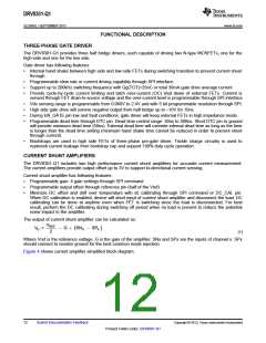
PROTECTION FEATURES
Power Stage Protection
The DRV8301-Q1 provides over-current and under-voltage protection for the MOSFET power stage. During fault
shut down conditions, all gate driver outputs will be kept low to ensure external FETs at high impedance state.
Over-Current Protection (OCP) and Reporting
To protect the power stage from damage due to high currents, a VDS sensing circuitry is implemented in the
DRV8301-Q1. Based on RDS(on) of the power MOSFETs and the maximum allowed IDS, a voltage threshold can
be calculated which, when exceeded, triggers the OC protection feature. This voltage threshold level is
programmable through SPI command.
There are total 4 OC_MODE settings in SPI.
1. Current Limit Mode
When current limit mode is enabled, device operates current limiting instead of OC shut down during OC
event. The over-current event is reported through OCTW pin. OCTW reporting should hold low during same
PWM cycle or for a max 64µs period (internal timer) so external controller has enough time to sample the
warning signal. If in the middle of reporting, other FET(s) gets OC, then OCTW reporting will hold low and
recount another 64µS unless PWM cycles on both FETs are ended.
There are two current control settings in current limit mode (selected by one bit in SPI and default is CBC
mode).
–
–
Setting 1 (CBC mode): during OC event, the FET that detected OC will turn off until next PWM cycle.
Setting 2 (off-time control mode):
–
During OC event, the FET that detected OC will turn off for 64us as off time and back to normal after
that (so same FET will be on again) if PWM signal is still holding high. Since all three phases or 6
FETs share a single timer, if more than one FET get OC, the FETs will not be back to normal until the
all FETs that have OC event pass 64µs.
–
–
If PWM signal is toggled for this FET during timer running period, device will resume normal operation
for this toggled FET. So real off-time could be less than 64uS in this case.
If two FETs get OC and one FET’s PWM signal gets toggled during timer running period, this FET will
be back to normal, and the other FET will be off till timer end (unless its PWM is also toggled)
14
Submit Documentation Feedback
Copyright © 2013, Texas Instruments Incorporated
Product Folder Links: DRV8301-Q1

 TI [ TEXAS INSTRUMENTS ]