DRV8301-Q1
SLOS842 –SEPTEMBER 2013
www.ti.com
SPI Pins
SDO pin has to be 3-state, so a data bus line can be connected to multiple SPI slave devices. SCS pin is active
low. When SCS is high, SDO is at high impendence mode.
STARTUP AND SHUTDOWN SEQUENCE CONTROL
During power-up all gate drive outputs are held low. Normal operation of gate driver and current shunt amplifiers
can be initiated by toggling EN_GATE from a low state to a high state. If no errors are present, the DRV8301-Q1
is ready to accept PWM inputs. Gate driver always has control of the power FETs even in gate disable mode as
long as PVDD is within functional region.
There is an internal diode from SDO to VDD_SPI, so VDD_SPI is required to be powered to the same power
level as other SPI devices (if there is any SDO signal from other devices) all the time. VDD_SPI supply should
be powered up first before any signal appears at SDO pin and powered down after completing all
communications at SDO pin.
SPI COMMUNICATION
SPI Interface
SPI interface is used to set device configuration, operating parameters and read out diagnostic information. The
DRV8301-Q1 SPI Interface operates in the slave mode.
The SPI input data (SDI) word consists of 16bit word, with 11 bit data and 5 bit (MSB) command. The SPI output
data (SDO) word consists of 16bit word, with 11 bit register data and 4 bit MSB address data and 1 frame fault
bit (active 1). When a frame is not valid, frame fault bit will set to 1, and rest of SDO bit will shift out zeros.
A valid frame has to meet following conditions:
1. Clock must be low when /SCS goes low.
2. We should have 16 full clock cycles.
3. Clock must be low when /SCS goes high.
When SCS is asserted high, any signals at the SCLK and SDI pins are ignored, and SDO is forced into a high
impedance state. When SCS transitions from HIGH to LOW, SDO is enabled and the SPI response word loads
into the shift register based on 5 bit command in SPI at previous clock cycle.
The SCLK pin must be low when SCS transitions low. While SCS is low, at each rising edge of the clock, the
response bit is serially shifted out on the SDO pin with MSB shifted out first.
While SCS is low, at each falling edge of the clock, the new control bit is sampled on the SDI pin. The SPI
command bits are decoded to determine the register address and access type (read or write). The MSB will be
shifted in first. If the word sent to SDI is less than 16 bits or more than 16 bits, it is considered a frame error. If it
is a write command, the data will be ignored. The fault bit in SDO (MSB) will report 1 at next 16 bit word cycle.
After the 16th clock cycle or when SCS transitions from LOW to HIGH, in case of write access type, the SPI
receive shift register data is transferred into the latch where address matches decoded SPI command address
value. Any amount of time may pass between bits, as long as SCS stays active low. This allows two 8-bit words
to be used.
For a read command (Nth cycle) in SPI, SP0 will send out data in the register with address in read command in
next cycle (N+1).
For a write command in SPI, SPO will send out data in the status register 0x00h in next 16 bit word cycle (N+1).
For most of the time, this feature will maximize SPI communication efficiency when having a write command, but
still get fault status values back without sending extra read command.
SPI Format
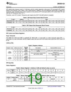
SPI input data control word is 16-bit long, consisting of:
•
•
•
1 read or write bit W [15]
4 address bits A [14:11]
11 data bits D [10:0]
18
Submit Documentation Feedback
Copyright © 2013, Texas Instruments Incorporated
Product Folder Links: DRV8301-Q1

 TI [ TEXAS INSTRUMENTS ]