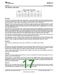
DRV8301-Q1
www.ti.com
SLOS842 –SEPTEMBER 2013
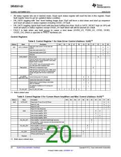
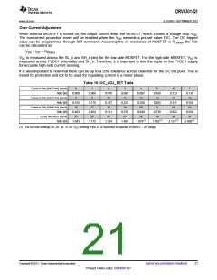
Over Current Adjustment
When external MOSFET is turned on, the output current flows the MOSFET, which creates a voltage drop VDS
.
The overcurrent protection event will be enabled when the VDS exceeds a pre-set value IOC. The OC tripped
value can be programmed through SPI command. Assuming the on resistance of MOSFET is RDS(on), the Vds
can be calculated as:
VDS = IOC × RDS(on)
VDS is measured across the SL_x and SH_x pins for the low-side MOSFET. For the high-side MOSFET, VDS is
measured across PVDD1 (internally) and SH_x. Therefore, it is important to limit the ripple on the PVDD1 supply
for accurate high-side current sensing.
It is also important to note that there can be up to a 20% tolerance across channels for the OC trip point. This is
meant for protection and not to be used for regulating current in a motor phase.
Table 10. OC_ADJ_SET Table
Control Bit (D6–D10) (0xH)
Vds (V)
0
1
2
3
4
0.097
12
5
0.109
13
6
0.123
14
7
0.138
15
0.060
8
0.068
9
0.076
10
0.086
11
Control Bit (D6–D10) (0xH)
Vds (V)
0.155
16
0.175
17
0.197
18
0.222
19
0.250
20
0.282
21
0.317
22
0.358
23
Control Bit (D6–D10) (0xH)
Vds (V)
0.403
24
0.454
25
0.511
26
0.576
27
0.648
28
1.679(1)
0.730
29
1.892(1)
0.822
30
2.131(1)
0.926
31
2.400(1)
Code Number (0xH)
Vds (V)
1.043
1.175
1.324
1.491
(1) Do not use settings 28, 29, 30, 31 for VDS sensing if the IC is expected to operate in the 6V – 8V range.
Copyright © 2013, Texas Instruments Incorporated
Submit Documentation Feedback
21
Product Folder Links: DRV8301-Q1

 TI [ TEXAS INSTRUMENTS ]