DM385, DM388
www.ti.com
NO.
SPRS821D –MARCH 2013–REVISED DECEMBER 2013
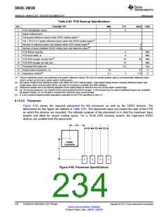
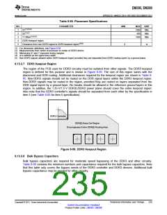
Table 8-65. Placement Specifications
PARAMETER
MIN
MAX
1000
600
UNIT
Mils
Mils
Mils
1
2
3
4
5
X1(1)(2)(3)
X2(1)(2)
Y Offset(1)(2)(3)
1500
DDR3 keepout region
Clearance from non-DDR3 signal to DDR3 keepout region(4)(5)
4
w
(1) For dimension definitions, see Figure 8-58.
(2) Measurements from center of processor to center of DDR3 device.
(3) Minimizing X1 and Y improves timing margins.
(4) w is defined as the signal trace width.
(5) Non-DDR3 signals allowed within DDR3 keepout region provided they are separated from DDR3 routing layers by a ground plane.
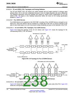
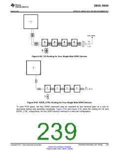
8.13.3.7 DDR3 Keepout Region
The region of the PCB used for DDR3 circuitry must be isolated from other signals. The DDR3 keepout
region is defined for this purpose and is shown in Figure 8-59. The size of this region varies with the
placement and DDR routing. Additional clearances required for the keepout region are shown in Table 8-
65. Non-DDR3 signals should not be routed on the DDR signal layers within the DDR3 keepout region.
Non-DDR3 signals may be routed in the region, provided they are routed on layers separated from the
DDR signal layers by a ground layer. No breaks should be allowed in the reference ground layers in this
region. In addition, the 1.35-V/1.5-V DDR3L/DDR3 power plane should cover the entire keepout region.
Also note that the DDR3 controller's signals should be separated from each other by the specification in
item 5 (see Table 8-65 for item 5 specification).
DDR3 Controller
DDR[0] Keep Out Region
Encompasses Entire DDR[0] Routing Area
Figure 8-59. DDR3 Keepout Region
8.13.3.8 Bulk Bypass Capacitors
Bulk bypass capacitors are required for moderate speed bypassing of the DDR3 and other circuitry.
Table 8-66 contains the minimum numbers and capacitance required for the bulk bypass capacitors. Note
that this table only covers the bypass needs of the DDR3 controller and DDR3 devices. Additional bulk
bypass capacitance may be needed for other circuitry.
Copyright © 2013, Texas Instruments Incorporated
Peripheral Information and Timings
235
Submit Documentation Feedback
Product Folder Links: DM385 DM388

 TI [ TEXAS INSTRUMENTS ]